Figure 16. control port timing, i·c read, 8 interrupts and overflow, Figure 16.control port timing, i²c read – Cirrus Logic CS5346 User Manual
Page 25: Figure 16, Cs5346
DS861PP3
25
CS5346
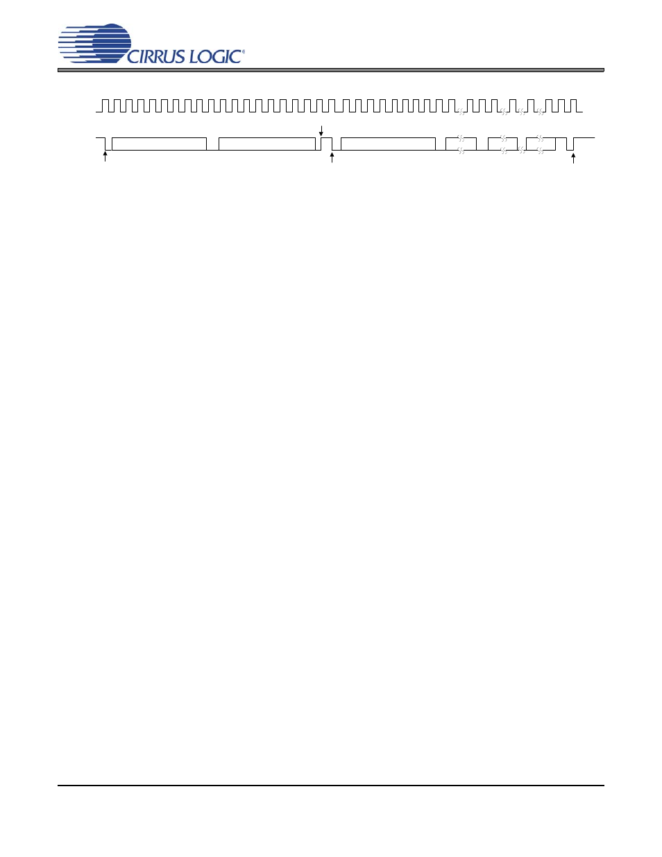
Since the read operation cannot set the MAP, an aborted write operation is used as a preamble. As shown
, the write operation is aborted after the acknowledge for the MAP byte by sending a stop con-
dition. The following pseudocode illustrates an aborted write operation followed by a read operation.
• Send start condition.
• Send 10011xx0 (chip address & write operation).
• Receive acknowledge bit.
• Send MAP byte.
• Receive acknowledge bit.
• Send stop condition, aborting write.
• Send start condition.
• Send 10011xx1(chip address & read operation).
• Receive acknowledge bit.
• Receive byte, contents of selected register.
• Send acknowledge bit.
• Send stop condition.
5.8
Interrupts and Overflow
The CS5346 has a comprehensive interrupt capability. The INT output pin is intended to drive the interrupt
input pin on the host microcontroller. The INT pin may function as either an active high CMOS driver or
an active-low, open-drain driver (see “Active High/Low (Bit 0)” on page 35). When configured as active
low open-drain, the INT pin has no active pull-up transistor, allowing it to be used for wired-OR hook-ups
with multiple peripherals connected to the microcontroller interrupt input pin. In this configuration, an ex-
ternal pull-up resistor must be placed on the INT pin for proper operation.
Many conditions can cause an interrupt, as listed in the interrupt status register descriptions (see “Inter-
rupt Status - Address 0Dh” on page 35). Each source may be masked off through mask register bits. In
addition, Each source may be set to rising edge, falling edge, or level-sensitive. Combined with the option
of level-sensitive or edge-sensitive modes within the microcontroller, many different configurations are
possible, depending on the needs of the equipment designer.
The CS5346 also has a dedicated overflow output. The OVFL pin functions as active low open drain and
has no active pull-up transistor, thereby requiring an external pull-up resistor. The OVFL pin outputs an
OR of the ADCOverflow and ADCUnderflow conditions available in the Interrupt Status register; however,
these conditions do not need to be unmasked for proper operation of the OVFL pin.
SCL
CHIP ADDRESS (WRITE)
MAP BYTE
DATA
DATA +1
START
ACK
STOP
ACK
ACK
ACK
1 0 0 1 1 AD1 AD0 0
SDA
1 0 0 1 1 AD1 AD0 1
CHIP ADDRESS (READ)
START
7 6 5 4 3 2 1 0
7 0
7 0
7 0
NO
16
8 9
12 13 14 15
4 5 6 7
0 1
20 21 22 23 24
26 27 28
2 3
10 11
17 18 19
25
ACK
DATA + n
STOP
Figure 16. Control Port Timing, I²C Read