Figure 10. cs5346 pga, Figure 11. 1 vrms input circuit, Figure 12. 1 vrms input circuit with rf filtering – Cirrus Logic CS5346 User Manual
Page 22: Figure 13. 2 vrms input circuit, Figure 10.cs5346 pga, Figure 11.1 v, Figure 12.1 v, Figure 13.2 v, Cs5346, 2 analog input configuration for 2 v
22
DS861PP3
CS5346
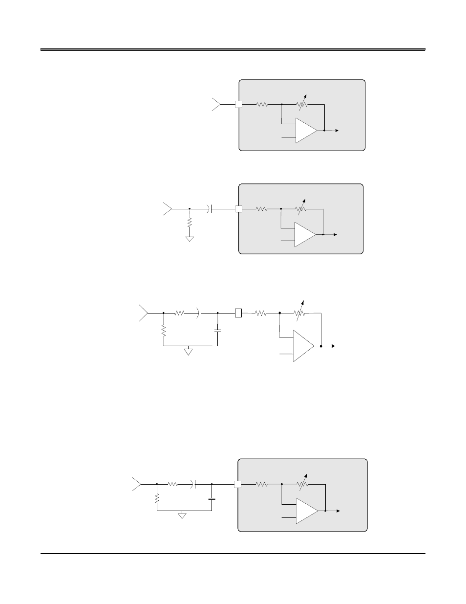
demonstrates a simple solution. The 1800 pF capacitors in the low-pass filter should be C0G or equivalent
to avoid distortion issues
.
5.5.2
Analog Input Configuration for 2 V
RMS
Input Levels
The CS5346 can also be easily configured to support an external 2 V
RMS
input signal, as shown in
Figure 13. In this configuration, the 2 V
RMS
input signal is attenuated to 1.5 V
RMS
at the analog input with
the external 12 k resistor and the input impedance to the network is increased to 48 k. The PGA gain
must also be configured to attenuate the 1.5 V
RMS
at the input pin to the 1.0 V
RMS
maximum A/D input level
to prevent clipping in the ADC.
36 k
V
CM
9 k to 144 k
A/ D Input
-
+
Analog Input
CS5346
Figure 10. CS5346 PGA
36 k
V
CM
9 k to 144 k
A/ D Input
-
+
2. 2 µF
100 k
Analog Input
CS5346
Figure 11. 1 V
RMS
Input Circuit
36 k
V
CM
9 k to 144 k
A/D Input
2.2 µF
1800 pF
100 k
100
-
+
Analog Input
Figure 12. 1 V
RMS
Input Circuit with RF Filtering
36 k
V
CM
9 k to 144 k
A/ D Input
-
+
2. 2 µF
18 pF
100 k
12 k
Analog Input
CS5346
Figure 13. 2 V
RMS
Input Circuit