Cirrus Logic CS5346 User Manual
Cs5346, Preliminary product information, Adc features
Copyright
Cirrus Logic, Inc. 2012
(All Rights Reserved)
Preliminary Product Information
This document contains information for a product under development.
Cirrus Logic reserves the right to modify this product without notice.
103-dB, 192-kHz, Stereo Audio ADC with 6:1 Input Mux
ADC Features
Multi-bit Delta–Sigma Modulator
103 dB Dynamic Range
-95 dB THD+N
Stereo 6:1 Input Multiplexer
Programmable Gain Amplifier (PGA)
– ± 12 dB Gain, 0.5-dB Step Size
– Zero-crossing, Click-free Transitions
Stereo Microphone Inputs
– +32 dB Gain Stage
– Low-noise Bias Supply
Up to 192 kHz Sampling Rates
Selectable 24-bit, Left-justified or I²S Serial
Audio Interface Formats
System Features
Power-down Mode
+5 V Analog Power Supply, Nominal
+3.3 V Digital Power Supply, Nominal
Direct Interface with 3.3 V to 5 V Logic Levels
Pin Compatible with CS5345 (*See
for details.)
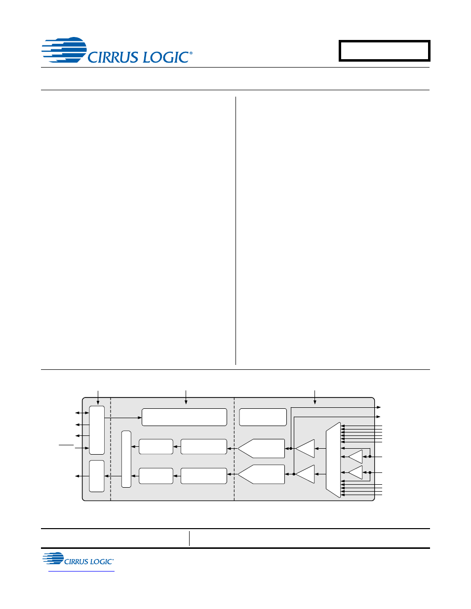
General Description
The CS5346 integrates an analog multiplexer, program-
mable gain amplifier, and stereo audio analog-to-digital
converter. The CS5346 performs stereo analog-to-digi-
tal (A/D) conve rsion of 24-bit serial values at sa mple
rates up to 192 kHz.
A 6:1 stereo input multiplexer is included for selecting
between line-level and microphone-level inputs. The
microphone input path includes a +32 dB gain stage
and a low-noise bias voltage supply. The PGA is avail-
able for line or microphone inputs and provides
gain/attenuation of ±12 dB in 0.5 dB steps.
The output of the PGA is followed by an advanced 5th-
order, multi-bit delta-sigma modulator and digital filter-
ing/decimation. Sampled data is transmitted by the
serial audio interface at rates from 8 kHz to 192 kHz in
either Slave or Master Mode.
Integrated level translators allow easy interfacing be-
tween the CS5346 and other devices operating over a
wide range of logic levels.
The CS5346 is available in a 48-pin LQFP package in
Commercial (-40° to +85° C) grade. The CDB5346 Cus-
tomer Demonstration board is also available for device
evaluation and implementation suggestions. Please re-
fer to
“Ordering Information” on page 38
for complete
details.
3.3 V to 5 V
Low-Latency
Anti-Alias Filter
Internal Voltage
Reference
Multibit
Oversampling
ADC
Multibit
Oversampling
ADC
Low-Latency
Anti-Alias Filter
High Pass
Filter
High Pass
Filter
Stereo Input 1
Serial
Audio
Output
3.3 V
5 V
MUX
PC
M
S
eri
al
In
te
rface
Register Configuration
Le
vel
Tran
slat
or
Stereo Input 2
Stereo Input 3
Stereo Input 4 /
Mic Input 1 & 2
Stereo Input 5
Stereo Input 6
PGA
+32 dB
+32 dB
Le
vel
T
ra
nslat
or
Reset
I²C
/SPI
Control Data
Interrupt
Overflow
Left PGA Output
Right PGA Output
PGAA
AUG ‘12
DS861PP3
CS5346
Document Outline
- 1. Pin Descriptions - CS5346
- 2. Pin Compatibility - cs5345/cs5346 Differences
- 3. Characteristics and Specifications
- Recommended Operating Conditions
- Absolute Maximum Ratings
- Analog Characteristics
- Analog Characteristics Cont.
- Digital Filter Characteristics
- DC Electrical Characteristics
- Digital Interface Characteristics
- Switching Characteristics - Serial Audio Port
- Switching Characteristics - Control Port - I·C Format
- Switching Characteristics - Control Port - SPI Format
- 4. Typical Connection Diagram
- 5. Applications
- 5.1 Recommended Power-Up Sequence
- 5.2 System Clocking
- 5.3 High-Pass Filter and DC Offset Calibration
- 5.4 Analog Input Multiplexer, PGA, and Mic Gain
- 5.5 Input Connections
- 5.6 PGA Auxiliary Analog Output
- 5.7 Control Port Description and Timing
- 5.8 Interrupts and Overflow
- 5.9 Reset
- 5.10 Synchronization of Multiple Devices
- 5.11 Grounding and Power Supply Decoupling
- 6. Register Quick Reference
- 7. Register Description
- 7.1 Chip ID - Register 01h
- 7.2 Power Control - Address 02h
- 7.3 ADC Control - Address 04h
- 7.4 MCLK Frequency - Address 05h
- 7.5 PGAOut Control - Address 06h
- 7.6 Channel B PGA Control - Address 07h
- 7.7 Channel A PGA Control - Address 08h
- 7.8 ADC Input Control - Address 09h
- 7.9 Active Level Control - Address 0Ch
- 7.10 Status - Address 0Dh
- 7.11 Status Mask - Address 0Eh
- 7.12 Status Mode MSB - Address 0Fh
- 7.13 Status Mode LSB - Address 10h
- 8. Parameter Definitions
- 9. Filter Plots
- Figure 17. Single-Speed Stopband Rejection
- Figure 18. Single-Speed Stopband Rejection
- Figure 19. Single-Speed Transition Band (Detail)
- Figure 20. Single-Speed Passband Ripple
- Figure 21. Double-Speed Stopband Rejection
- Figure 22. Double-Speed Stopband Rejection
- Figure 23. Double-Speed Transition Band (Detail)
- Figure 24. Double-Speed Passband Ripple
- Figure 25. Quad-Speed Stopband Rejection
- Figure 26. Quad-Speed Stopband Rejection
- Figure 27. Quad-Speed Transition Band (Detail)
- Figure 28. Quad-Speed Passband Ripple
- 10. Package Dimensions
- 11. Thermal Characteristics and Specifications
- 12. Ordering Information
- 13. Revision History