4 analog input multiplexer, pga, and mic gain, Figure 9. analog input architecture, 5 input connections – Cirrus Logic CS5346 User Manual
Page 21: Figure 9.analog input architecture, Cs5346, 1 analog input configuration for 1 v, Input levels
DS861PP3
21
CS5346
5.4
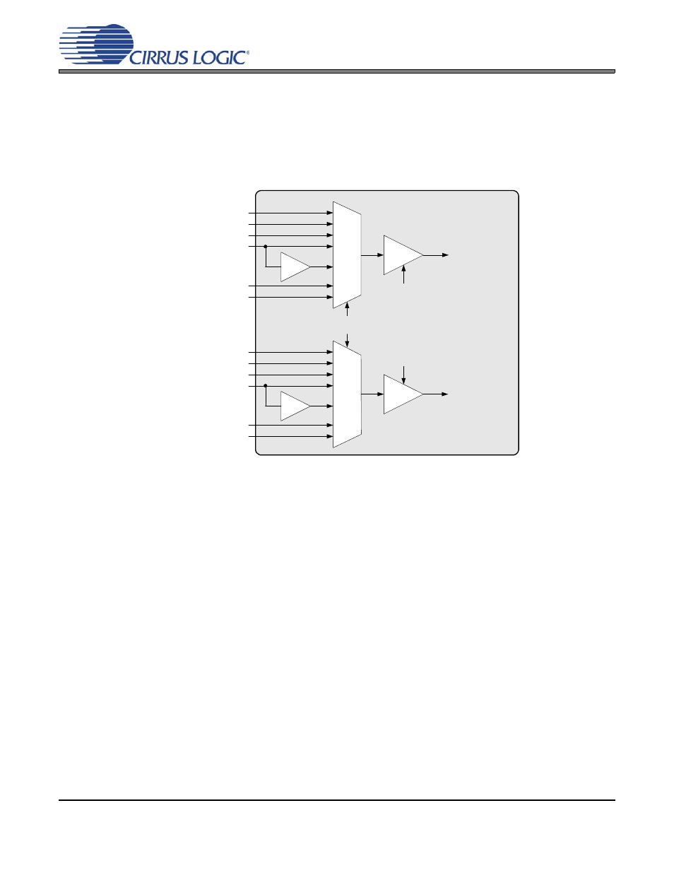
Analog Input Multiplexer, PGA, and Mic Gain
The CS5346 contains a stereo 6-to-1 analog input multiplexer followed by a programmable gain amplifier
(PGA). The input multiplexer can select one of six possible stereo analog input sources and route it to the
PGA. Analog inputs 4A and 4B are able to insert a +32 dB (+40x) gain stage before the input multiplexer,
allowing them to be used for microphone-level signals without the need for any external gain. The PGA
stage provides 12 dB (4x) adjustment in 0.5 dB steps.
shows the architecture of the input multi-
plexer, PGA, and microphone gain stages.
The “
“Analog Input Selection (Bits 2:0)” on page 32
” outlines the bit settings necessary to control the input
multiplexer and mic gain.
“Channel B PGA Control - Address 07h” on page 30
and
outline the register settings necessary to control the PGA. By default, line-
level input 1 is selected, and the PGA is set to 0 dB.
5.5
Input Connections
The analog modulator samples the input at 6.144 MHz (MCLK=12.288 MHz). The digital filter will reject sig-
nals within the stopband of the filter. However, there is no rejection for input signals
which are
(n
6.144 MHz) the digital passband frequency, where n=0,1,2,... Refer to the Typical Connection Diagram
for the recommended analog input circuit that will attenuate noise energy at 6.144 MHz. The use of capac-
itors which have a lar ge voltage coefficient (such as ge neral-purpose ceramics) must be avoided since
these can degrade signal linearity. Any unused analog input pairs should be left unconnected.
5.5.1
Analog Input Configuration for 1 V
RMS
Input Levels
The CS5346 PGA, excluding the input multiplexer, is shown in Figure 10 with nominal component values.
Interfacing to this circuit is a relatively simple matter and several options are available. The simplest option
is shown in Figure 11. However, it may be advantageous in some applications to provide a low-pass filter
prior to the PGA to prevent radio frequency interference within the amplifier. The circuit shown in Figure 12
MUX
+32 dB
AIN1A
AIN2A
AIN3A
AIN4A/MICIN1
AIN5A
AIN6A
PGA
MUX
+32 dB
AIN1B
AIN2B
AIN3B
AIN4B/MICIN2
AIN5B
AIN6B
Analog Input
Selection Bits
Channel A
PGA Gain Bits
Channel B
PGA Gain Bits
Out to ADC
Channel A
Out to ADC
Channel B
PGA
Figure 9. Analog Input Architecture