Figure 14. control port timing in spi mode, 2 i·c mode, Figure 15. control port timing, i·c write – Cirrus Logic CS5346 User Manual
Page 24: 2 i²c mode, Figure 14.control port timing in spi mode, Figure 15.control port timing, i²c write, Figure 14, Cs5346
24
DS861PP3
CS5346
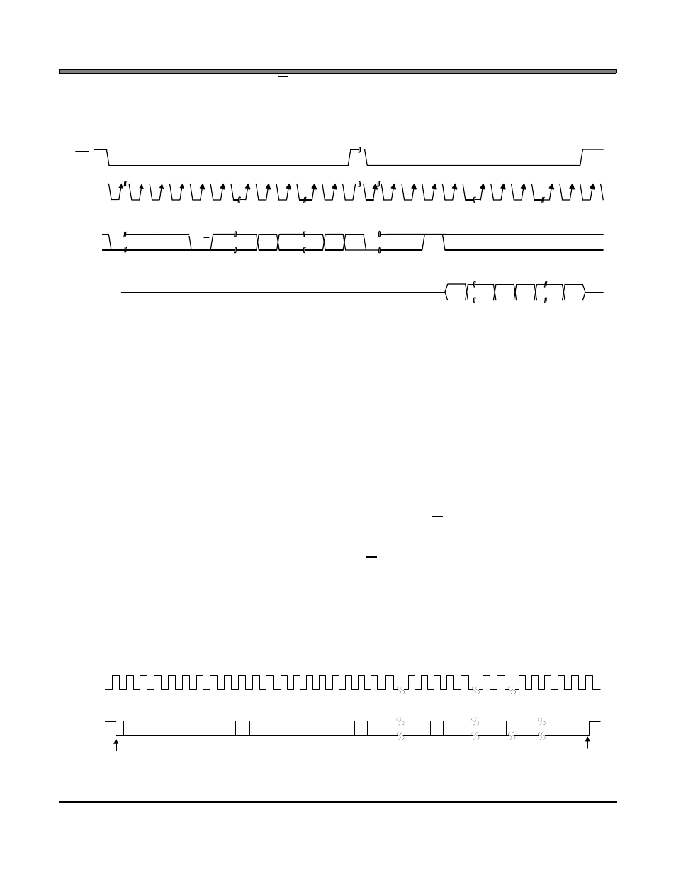
dress and set the read/write bit (R/W) high. The next falling edge of CCLK will clock out the MSB of the
addressed register (CDOUT will leave the high-impedance state).
For both read and write cycles, the memory address pointer will automatically increment following each
data byte in order to facilitate block reads and writes of successive registers.
5.7.2
I²C Mode
In I²C Mode, SDA is a bidirectional data line. Data is clocked into and out of the part by the clock, SCL.
There is no CS pin. Pins AD0 and AD1 form the two least-significant bits of the chip address and should
be connected through a resistor to VLC or DGND as desired. The state of the pins is sensed while the
CS5346 is being reset.
The signal timings for a read and write cycle are shown in
and
. A Start condition is
defined as a falling transition of SDA while the clock is high. A Stop condition is a rising transition while
the clock is high. All other transitions of SDA occur while the clock is low. The first byte sent to the CS5346
after a Start condition consists of a 7-bit chip address field and a R/W bit (high for a read, low for a write).
The upper 5 bits of the 7-bit address field are fixed at 10011. To communicate with a CS5346, the chip
address field, which is the first byte sent to the CS5346, should match 10011 followed by the settings of
the AD1 and AD0. The 8th bit of the address is the R/W bit. If the operation is a write, the next byte is the
Memory Address Pointer (MAP) which selects the register to be read or written. If the operation is a read,
the contents of the register pointed to by the MAP will be output. Following each data byte, the memory
address pointer will automatically increment to facilitate block reads and writes of successive registers.
Each byte is separated by an acknowledge bit. The ACK bit is output from the CS5346 after each input
byte is read, and is input to the CS5346 from the microcontroller after each transmitted byte.
M A P
MSB
LSB
DATA
b y te 1
b y te n
R/W
R/W
A D D R E S S
C H IP
ADDRESS
C H IP
C D IN
C C L K
CS
C D O U T
MSB
LSB MSB
LSB
1001111
1001111
MAP = Memory Address Pointer, 8 bits, MSB first
High Impedance
Figure 14. Control Port Timing in SPI Mode
4 5 6 7
24 25
SCL
CHIP ADDRESS (WRITE)
MAP BYTE
DATA
DATA +1
START
ACK
STOP
ACK
ACK
ACK
1 0 0 1 1 AD1 AD0 0
SDA
6 6 5 4 3 2 1 0
7 6 1 0
7 6 1 0
7 6 1 0
0 1 2 3
8 9
12
16 17 18 19
10 11
13 14 15
27 28
26
DATA +n
Figure 15. Control Port Timing, I²C Write