Figure 6. control port timing - spi format, Figure 6.control port timing - spi format – Cirrus Logic CS5346 User Manual
Page 17
DS861PP3
17
CS5346
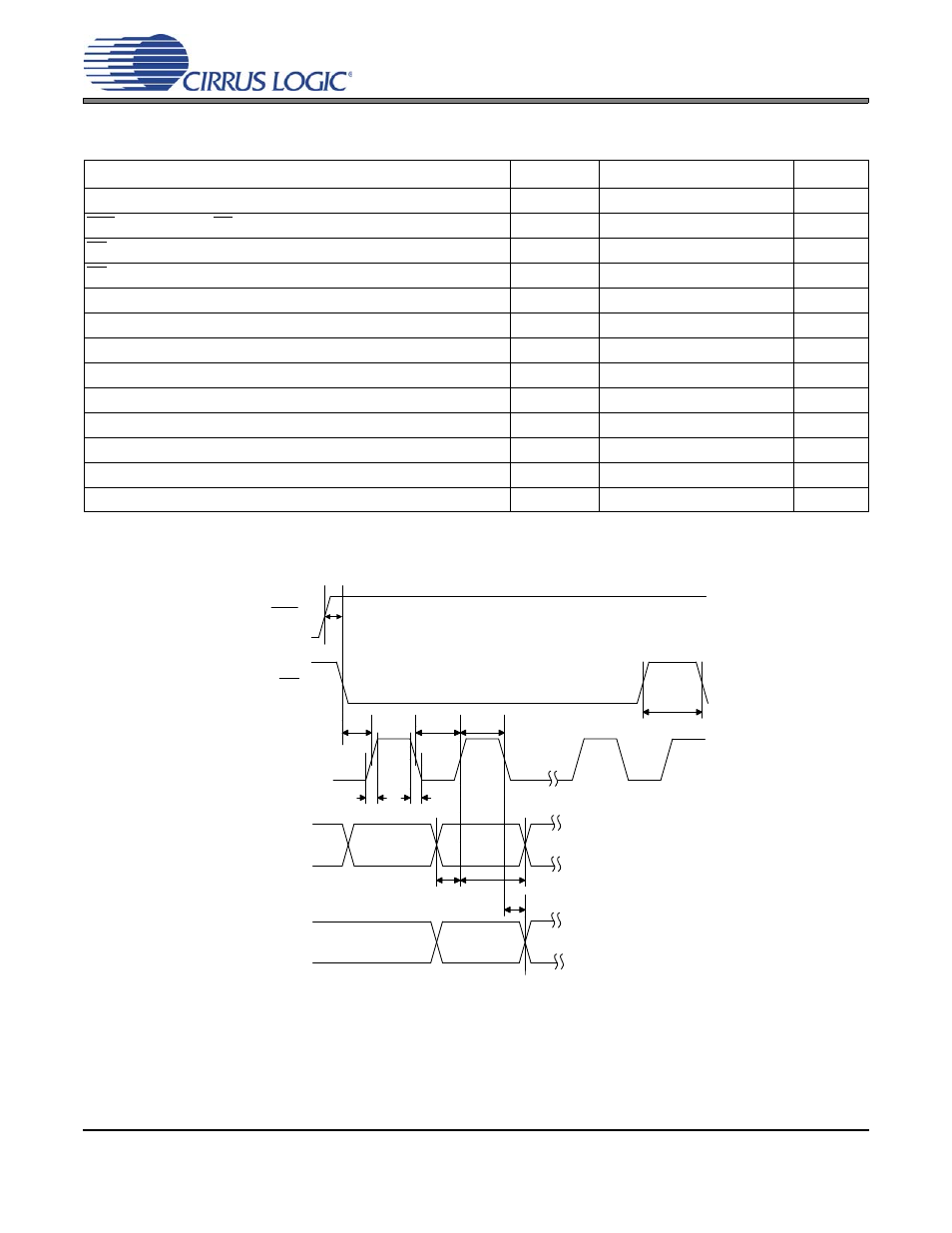
SWITCHING CHARACTERISTICS - CONTROL PORT - SPI FORMAT
Inputs: Logic 0 = DGND = AGND = 0 V, Logic 1 = VLC, C
L
= 30 pF.
14. Data must be held for sufficient time to bridge the transition time of CCLK.
15. For f
sck
<1 MHz.
Parameter
Symbol
Min
Max
Units
CCLK Clock Frequency
f
sck
-
6.0
MHz
RST Rising Edge to CS Falling
t
srs
500
-
ns
CS High Time Between Transmissions
t
csh
1.0
-
s
CS Falling to CCLK Edge
t
css
20
-
ns
CCLK Low Time
t
scl
66
-
ns
CCLK High Time
t
sch
66
-
ns
CDIN to CCLK Rising Setup Time
t
dsu
40
-
ns
CCLK Rising to DATA Hold Time
t
dh
15
-
ns
CCLK Falling to CDOUT Stable
t
pd
-
50
ns
Rise Time of CDOUT
t
r1
-
25
ns
Fall Time of CDOUT
t
f1
-
25
ns
Rise Time of CCLK and CDIN
t
r2
-
100
ns
Fall Time of CCLK and CDIN
t
f2
-
100
ns
t r2
t f2
t dsu
t dh
t sch
t scl
CS
CCLK
CDIN
t css
t pd
CDOUT
tcsh
RST
t srs
Figure 6. Control Port Timing - SPI Format
- CobraNet (147 pages)
- CS4961xx (54 pages)
- CS150x (8 pages)
- CS1601 (2 pages)
- CS1501 (16 pages)
- CS1601 (16 pages)
- CS1610 (16 pages)
- CRD1610-8W (24 pages)
- CRD1611-8W (25 pages)
- CDB1610-8W (21 pages)
- CS1610A (18 pages)
- CDB1611-8W (21 pages)
- CDB1610A-8W (21 pages)
- CDB1611A-8W (21 pages)
- CRD1610A-8W (24 pages)
- CRD1611A-8W (25 pages)
- CS1615 (16 pages)
- AN403 (15 pages)
- AN401 (14 pages)
- AN400 (15 pages)
- AN375 (27 pages)
- AN376 (9 pages)
- CRD1615-8W (22 pages)
- CRD1616-8W (23 pages)
- AN402 (14 pages)
- AN404 (15 pages)
- CRD1615A-8W (21 pages)
- CS1615A (16 pages)
- CS1630 (56 pages)
- AN374 (35 pages)
- AN368 (80 pages)
- CRD1630-10W (24 pages)
- CRD1631-10W (25 pages)
- CS1680 (16 pages)
- AN405 (13 pages)
- AN379 (31 pages)
- CRD1680-7W (31 pages)
- AN335 (10 pages)
- AN334 (6 pages)
- AN312 (14 pages)
- AN Integrating CobraNet into Audio Products (16 pages)
- CobraNet Audio Routing Primer (9 pages)
- Bundle Assignments in CobraNet Systems (3 pages)
- CS2300-01 (3 pages)
- CS2000-CP (38 pages)