1 stereo output, Figure 31. stereo output, 2 mono output – Cirrus Logic CS4205 User Manual
Page 66: 3 miscellaneous analog signals, 4 power supplies, Figure 32. +5v analog voltage regulator, 1 stereo output 12.2.2 mono output, 3 miscellaneous analog signals 12.4 power supplies, Cs4205

CS4205
66
DS489PP4
ence, nominally 2.4 V. This requires the outputs be
AC-coupled to external circuitry (AC loads must
be greater than 10 k
Ω for the line output).
12.2.1
Stereo Output
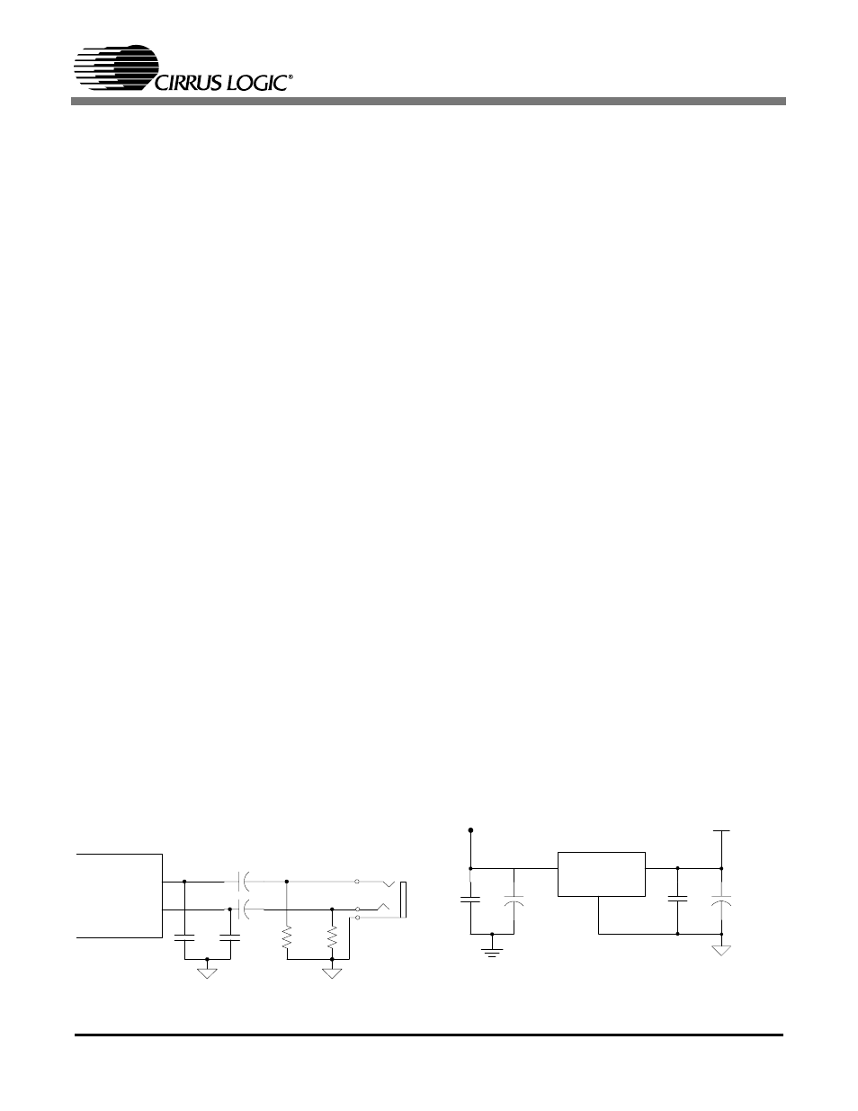
See Figure 31 for a stereo line-level output refer-
ence design.
12.2.2
Mono Output
The mono output, MONO_OUT, can be either a
sum of the left and right output channels, attenuat-
ed by 6 dB to prevent clipping at full scale, or the
selected Mic signal. The mono out channel can
drive the PC internal mono speaker using an appro-
priate buffer circuit.
12.3
Miscellaneous Analog Signals
The AFLT1, AFLT2, and AFLT3 pins must have a
1000 pF NPO capacitor to analog ground. These
capacitors provide a single-pole low-pass filter at
the inputs to the ADCs. This makes low-pass filters
at each analog input pin unnecessary.
The REFFLT pin must have a short, wide trace to a
2.2
µF and a 0.1 µF capacitor connected to analog
ground (see Figure 33 in Section 13, Grounding
and Layout, for an example). The 2.2
µF capacitor
must not be replaced by any other value (it may be
replaced with two 1 µF capacitors in parallel) and
must be ceramic with low leakage current. Electro-
lytic capacitors should not be used. No other con-
nection should be made, as any coupling onto this
pin will degrade the analog performance of the
CS4205. Likewise, digital signals should be kept
away from REFFLT for similar reasons.
12.4
Power Supplies
The power supplies providing analog power should
be as clean as possible to minimize coupling into
the analog section which could degrade analog per-
formance. The +5 V analog supply should be gen-
erated from a voltage regulator (7805 type)
connected to a +12 V supply. This helps isolate the
analog circuitry from noise typically found on +5 V
digital supplies. A typical voltage regulator circuit
for analog power using an MC78M05CDT is
shown in Figure 32. The AVdd1/AVss1 analog
power/ground pin pair on the CS4205 supplies
power to all the analog circuitry and should be con-
nected to +5 VA/AGND. The AVdd2 and AVss2
pins are not used on the CS4205 and may be left
floating or tied to +5 VA/AGND for backwards
compatibility.
The DVdd2/DVss2 digital power/ground pin pair
on the CS4205 should be connected to the same
digital supply as the controller’s AC-link interface.
Since the digital interface on the CS4205 may op-
erate at either +3.3 V or +5 V, proper connection of
these pins will depend on the digital power supply
of the controller. The DVdd1/DVss1 pair supplies
power to the clocking circuitry and needs to be con-
nected to the +5 VA/AGND power supply when
the CS4205 is in PLL clocking mode. In XTAL or
OSC clocking modes these pins may be connected
to either +5 VA/AGND or use the same power sup-
ply used for DVdd2/DVss2.
LINE_OUT_R
LINE_OUT_L
10
µF
ELEC
10
µF
ELEC
220 k
Ω
220 k
Ω
AGND
1000 pF
1000 pF
AGND
+
+
Line Out
Figure 31. Stereo Output
3
2
1
AGND
GND
IN
OUT
MC78M05CDT
+12VD
10
µF
ELEC
+
0.1
µF
Y5V
10
µF
ELEC
+
0.1
µF
Y5V
DGND
+5VA
Figure 32. +5V Analog Voltage Regulator
