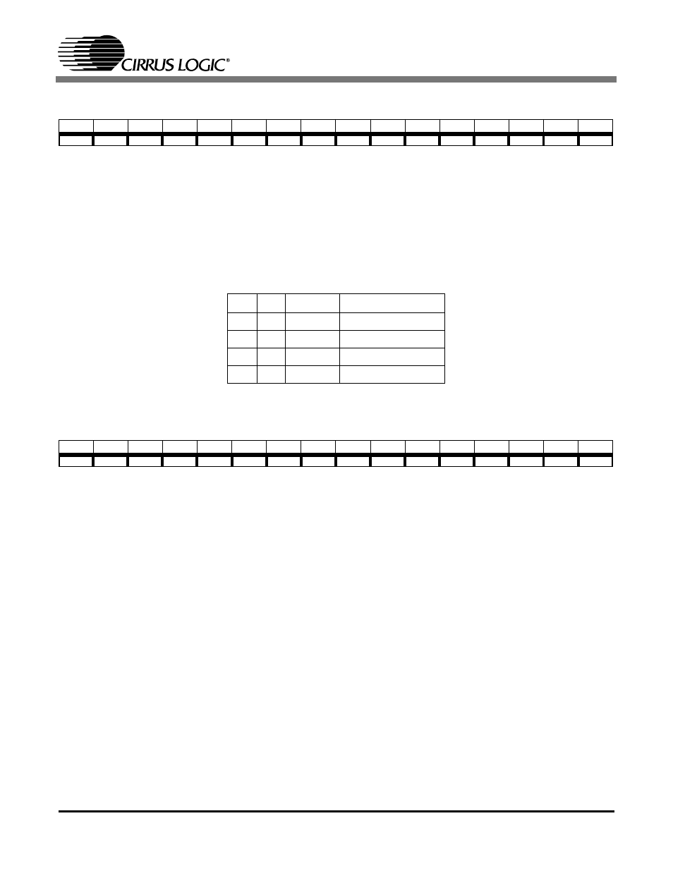
Table 13. gpio input/output configurations, Cs4205 – Cirrus Logic CS4205 User Manual
Page 40

CS4205
40
DS489PP4
5.21
GPIO Pin Polarity/Type Configuration Register (Index 4Eh)
GP[4:0]
GPIO Pin Configuration. This register defines the GPIO input polarity (0 = Active Low,
1 = Active High) when a GPIO pin is configured as an input. The GP[4:0] bits define the GPIO
output type (0 = CMOS, 1 = OPEN-DRAIN) when a GPIO pin is configured as an output. The
GC[4:0] bits in the GPIO Pin Configuration Register (Index 4Ch) define the GPIO pins as in-
puts or outputs. See Table 13 for the various GPIO configurations.
Default
FFFFh
After a Cold Reset or a modem Register Reset this register defaults to all 1’s. The upper 11 bits of this register al-
ways return ‘1’.
5.22
GPIO Pin Sticky Register (Index 50h)
GS[4:0]
GPIO Pin Sticky. This register defines the GPIO input type (0 = not sticky, 1 = sticky) when a
GPIO pin is configured as an input. The GPIO pin status of an input configured as “sticky” is
‘cleared’ by writing a ‘0’ to the corresponding bit of the GPIO Pin Status Register (Index 54h),
and by reset.
Default
0000h
After a Cold Reset or a modem Register Reset this register defaults to all 0’s, specifying “non-sticky”. “Sticky” is de-
fined as edge sensitive, “non-sticky” as level sensitive. The upper 11 bits of this register always return ‘0’.
D15
D14
D13
D12
D11
D10
D9
D8
D7
D6
D5
D4
D3
D2
D1
D0
1
1
1
1
1
1
1
1
1
1
1
GP4
GP3
GP2
GP1
GP0
GCx GPx Function
Configuration
0
0
Output
CMOS Drive
0
1
Output
Open Drain
1
0
Input
Active Low
1
1
Input
Active High (default)
Table 13. GPIO Input/Output Configurations
D15
D14
D13
D12
D11
D10
D9
D8
D7
D6
D5
D4
D3
D2
D1
D0
0
0
0
0
0
0
0
0
0
0
0
GS4
GS3
GS2
GS1
GS0
