Mode control register (index 5eh), Cs4205, 23 gpio pin wakeup mask register (index 52h) – Cirrus Logic CS4205 User Manual
Page 41: 24 gpio pin status register (index 54h), 25 ac mode control register (index 5eh)

CS4205
DS489PP4
41
5.23
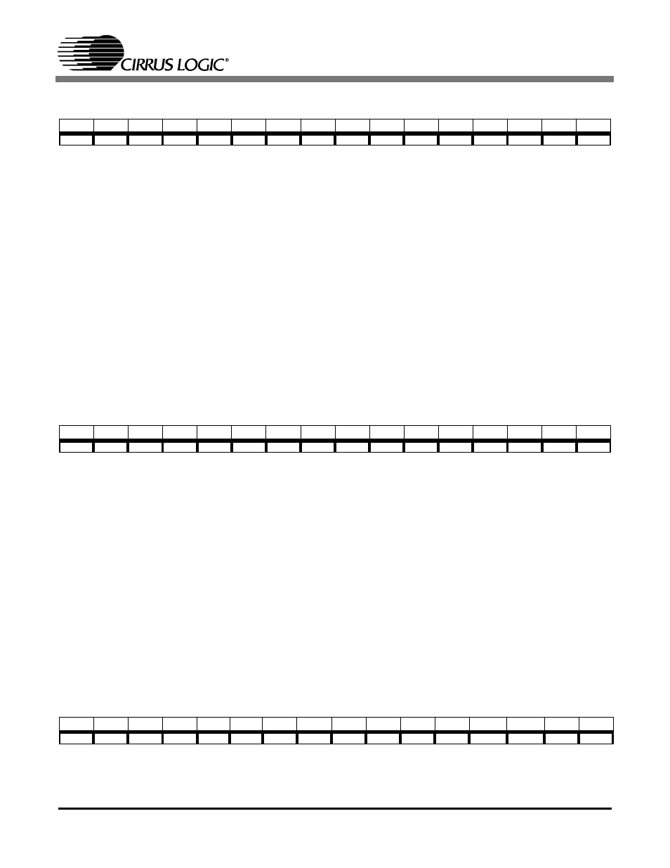
GPIO Pin Wakeup Mask Register (Index 52h)
GW[4:0]
GPIO Pin Wakeup. This register provides a mask for determining if an input GPIO change will
generate a wakeup event (0 = no, 1 = yes). When the AC-link is powered up, a wakeup event
will be communicated through the assertion of GPIO_INT = 1 in input Slot 12. When the
AC-link is powered down (Powerdown Control/Status Register (Index 26h) bit PR4 = 1 for pri-
mary codecs), a wakeup event will be communicated through a ‘0’ to ‘1’ transition on
SDATA_IN.
Default
0000h
GPIO bits which have been programmed as inputs, “sticky”, and “wakeup”, upon transition either (high-to-low) or
(low-to-high) depending on pin polarity, will cause an AC-link wakeup if and only if the AC-link was powered down.
Once the controller has re-established communication with the CS4205 following a Warm Reset, it will continue to
signal the wakeup event through the GPIO_INT bit of input Slot 12 until the AC ’97 controller clears the inter-
rupt-causing bit in the GPIO Pin Status Register (Index 54h); or the “wakeup”, config, or “sticky” status of that GPIO
pin changes.
After a Cold Reset or a modem Register Reset (see Extended Modem ID Register (Index 3Ch)) this register defaults
to all 0’s, specifying no wakeup event. The upper 11 bits of this register always return ‘0’.
5.24
GPIO Pin Status Register (Index 54h)
GI[4:0]
GPIO Pin Status. This register reflects the state of all GPIO pin inputs and outputs. These
values are also reflected in Slot 12 of every SDATA_IN frame. GPIO inputs configured as
“sticky” are ‘cleared’ by writing a ‘0’ to the corresponding bit of this register. The GPIO_INT
bit in input Slot 12 is ‘cleared’ by clearing all interrupt-causing bits in this register.
Default
0000h
GPIO pins which have been programmed as inputs and “sticky”, upon transition either (high-to-low) or (low-to-high)
depending on pin polarity, will cause the individual GI bit to be ‘set’, and remain ‘set’ until ‘cleared’. GPIO pins which
have been programmed as outputs are controlled either through output Slot 12 or through this register, depending
on the state of the GPOC bit in the Misc. Crystal Control Register (Index 60h). If the GPOC bit is ‘cleared’, the GI
bits in this register are read-only and reflect the status of the corresponding GPIO output pin ‘set’ through output
slot 12. If the GPOC bit is ‘set’, the GI bits in this register are read/write bits and control the corresponding GPIO
output pins.
The default value is always the state of the GPIO pin. The upper 11 bits of this register should be forced to zero in
this register and input Slot 12.
5.25
AC Mode Control Register (Index 5Eh)
DACS
DAC Source Select. The DACS bit controls the source of data routed to the DACs. If this bit
is ‘clear’, the DACs will receive data from the DAC slots, see Table 14 for actual slots used.
If this bit is ‘set’, the DACs will receive data from the CS4205 digital effects engine.
D15
D14
D13
D12
D11
D10
D9
D8
D7
D6
D5
D4
D3
D2
D1
D0
0
0
0
0
0
0
0
0
0
0
0
GW4
GW3
GW2
GW1
GW0
D15
D14
D13
D12
D11
D10
D9
D8
D7
D6
D5
D4
D3
D2
D1
D0
0
0
0
0
0
0
0
0
0
0
0
GI4
GI3
GI2
GI1
GI0
D15
D14
D13
D12
D11
D10
D9
D8
D7
D6
D5
D4
D3
D2
D1
D0
DACS CAPS1 CAPS0 MICS
0
0
TMM
DDM
AMAP
0
SM1
SM0
SDOS1 SDOS0 SPDS1 SPDS0
