3analog input / output, Internal schematic, 3 internal schematic – Horner APG RCX HE500RCX404 User Manual
Page 4
PAGE 4
23 MAR 2003
MAN0504-02
OCX404
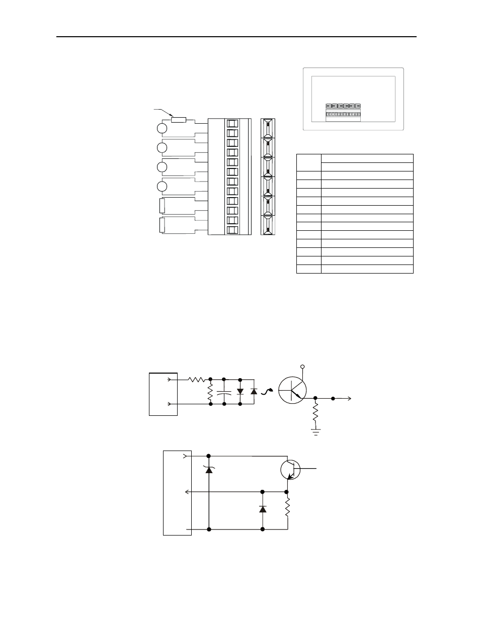
2.3
Analog Input / Output
OCX Back View Connector – Shows
corresponding I/O pin location
*
*
±10V LOAD
±20mA LOAD/RECEIVER
±10V SOURCE
±10V SOURCE
±20mA SELF POWERED TRANSMITTER
LOOP POWERED TRANSMITTER
+
+
20mA LOOP POWER
I1
C
I2
C
I3
C
I4
C
Q1
C
Q2
C
Signal
Pin
OCX404 Analog In / Out
I1 Input
1
C Common
I2 Input
2
C Common
I3 Input
3
C Common
I4 Input
4
C Common
I5 Input
5
C Common
I6 Input
6
C Common
001OCX005
Note: The Voltage/Current mode switch is located directly
above each input. Moving a switch towards Pin 1* selects
±20mA for the corresponding channel. Moving the switch
towards Pin 12 selects
±10VDC. Each channel must be set
up in Cscape for the desired mode in addition to the physical
switch settings for proper signal scaling in the PLC registers.
3 INTERNAL
SCHEMATIC
Mini Digital Input
C
iI1
I/O Connector
To
Controller
VCC
Field
Side
I/O Connector
Mini Digital Output
VC
Q
V+
From
Controller
Field
Side
Specification for transient voltage suppressors used on digital output circuitry is 33V, 300W.
Information is subject to change without notice. Cscape is a trademark of Horner APG, LLC.