Horner APG XL10e OCS Built-in I/O Model 5 I/O User Manual
Page 2

MAN0953-02-EN
Specifications / Installation
1/6/2011
Page 2 of 4
Negative Logic
Positive Logic
JP1 Digital DC Inputs
Default
2.1
I/O Jumper Settings
3
Digital Input Wiring Details
5
Analog I/O Wiring Details
4
Digital Output Wiring Details
Positive Logic In Negative Logic In
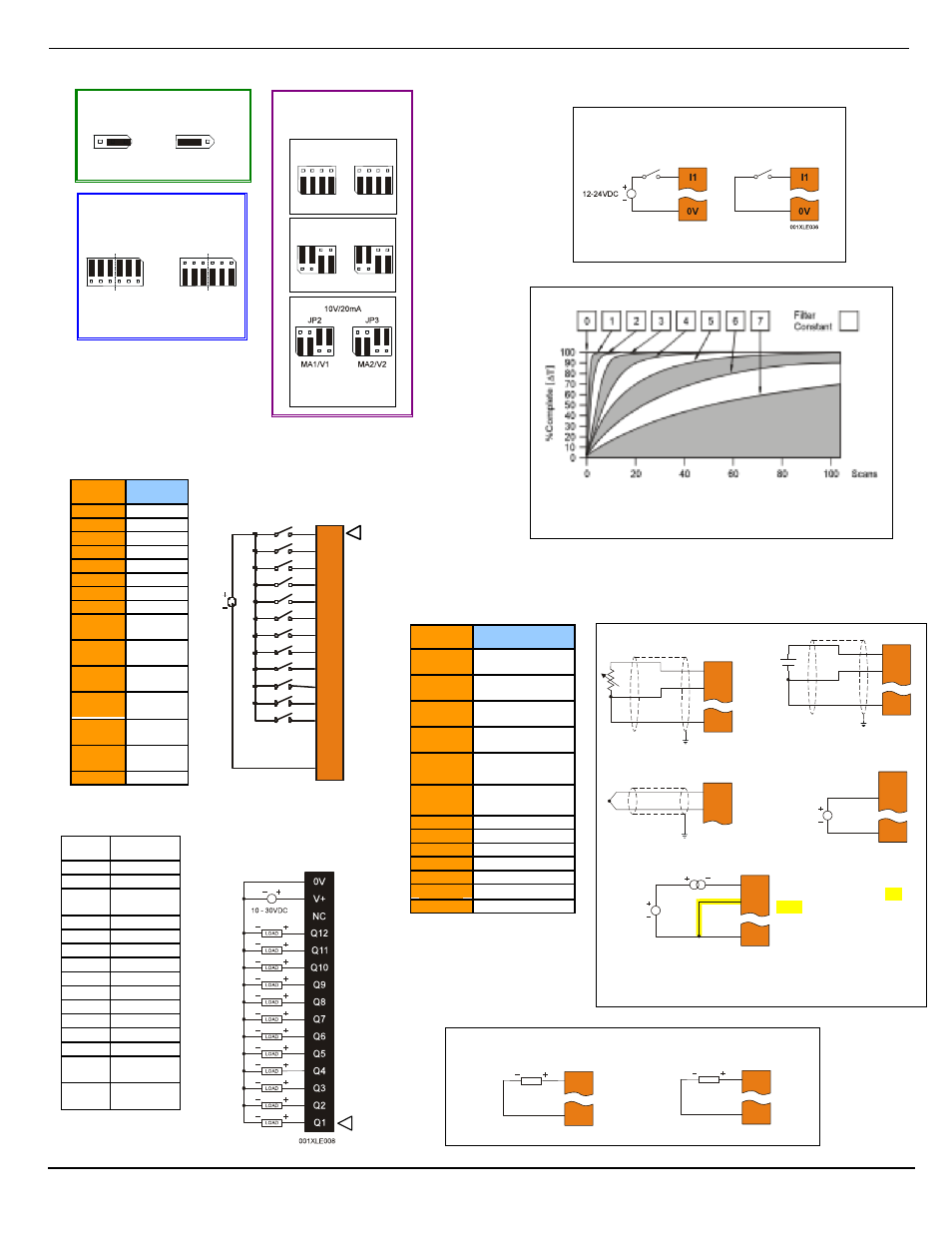
Positive Logic vs. Negative Logic Wiring
The XLe can be wired for Positive Logic inputs or
Negative Logic inputs.
The chart above demonstrates the effect of digital filtering on an analog
input value. The Digital Filtering level is set in Cscape as part of the I/O
Configuration.
Analog Input Digital Filtering
Analog In Settings
AI1 AI2
JP2
JP3
RTD (PT100)
T1
T2
JP2
JP3
T/C/100mV
T1
T2
Default
JP2 and JP3
CURRENT
(20mA)
VOLTAGE
(10V)
JP4
ANALOG OUTPUT SETTING
VOLTAGE OR CURRENT
AQ2
AQ1
AQ2
AQ1
Default
Note: When using JP4 (output) or
JP2 / JP3 (inputs), each channel can
be independently configured. For
example, JP2 can be configured for
10 V and JP3 can be configured as an
RTD.
J1
Orange
Name
I1
IN1
I2
IN2
I3
IN3
I4
IN4
I5
IN5
I6
IN6
I7
IN7
I8
IN8
H1
HSC1 /
IN9
H2
HSC2 /
IN10
H3
HSC3 /
IN11
H4
HSC4 /
IN12
NC
No
Connect
NC
No
Connect
0V
Ground
I1
I2
I3
I4
H2
H3
H4
0V
I5
I6
I7
I8
NC
NC
H1
001XLE007
12-24
VDC
J1 Orange
Positive Logic
Digital In
J2 Black
Positive Logic
Digital Outputs
J2
Black
Name
0V
Ground
V+*
V+*
NC
No
Connect
Q12
OUT12
Q11
OUT11
Q10
OUT10
Q9
OUT9
Q8
OUT8
Q7
OUT7
Q6
OUT6
Q5
OUT5
Q4
OUT4
Q3
OUT3
Q2
OUT2 /
PWM2
Q1
OUT1 /
PWM1
J2 Black
Positive Logic
Digital Outputs
J3
Orange
Name
T1+
T/C / RTD IN1+ /
100 mV+
T1-
T/C / RTD IN1- /
100 mV-
T2+
T/C / RTD IN2+ /
100 mV+
T2-
T/C / RTD IN2- /
100 mV-
AQ1
10 V / 20 mA
OUT1
*
AQ2
0 V / 20 mA
OUT2
*
0V
Ground
MA1
20 mA IN1
V1
10 V IN1
0V
Ground
MA2
20 mA IN2
V2
10 V IN2
0V
Ground
0 -10 V Analog Out
AQ1
0V
10VDC
4 - 20 mA Analog Out
AQ1
0V
20mA
Thermocouple In
T1+
T1-
0 – 10 V Analog In
0-10VDC
MA1
V1
0V
NC
RTD In
T1+
T1-
0V
Thermocouple In
T1+
T1-
RTD In
T1+
T1-
0V
mV In
T1+
T1-
0V
100mV+
100mV-
Note: Be sure to wire 0 V
to V1 as shown for proper
operation.
LOOP PWR
20mA
MA1
V1
0V
20 mA Analog In
0 – 10 V Analog In
0-10VDC
MA1
V1
0V
NC
0 -10 V Analog Out
AQ1
0V
10VDC
4 - 20 mA Analog Out
AQ1
0V
20mA
* IMPORTANT: the two analog
outputs are referenced at
registers %AQ9 & %AQ10 in
the application program
Note:
Loop Power requirements are determined by the
transmitter specification.
