Zxbm1021, Electrical characteristics – Diodes ZXBM1021 User Manual
Page 6
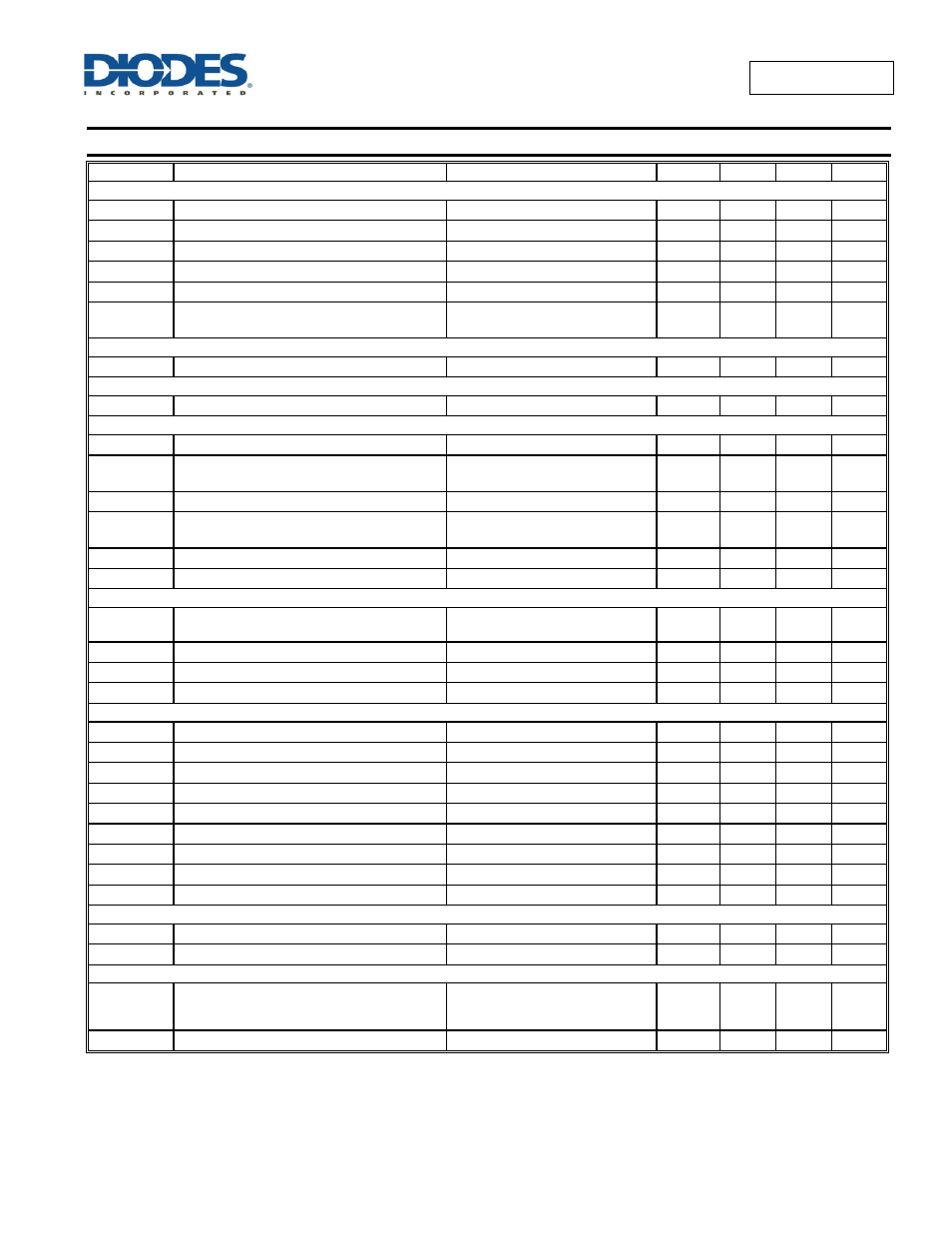
ZXBM1021
Document number: DS36322 Rev. 2 - 2
6 of 25
April 2014
© Diodes Incorporated
ZXBM1021
Electrical Characteristics
(cont.) (@T
A
= +25°C, V
DD
= 12V, unless otherwise specified.)
Symbol
Characteristics
Conditions
Min
Typ
Max
Unit
PWM Speed Control
V
PWMSPDH
PWMSPD High Level
2
V
CC
V
V
PWMSPDL
PWMSPD Low Level
0.4
V
I
PWMSPD
PWMSPD High Level Input Current
0.8
2
µA
D
PWMSPD
PWM Speed Signal Duty Range
0
100
%
F
PWM_MAX
Maximum Frequency of PWM Control Signal
100
kHz
Lin
INT
PWMSPD Pin PWM Duty Ratio to C
SPD
Output
Voltage Linearity
PWMSPD duty ratio 50%,
PWM frequency F
PWM
= 25kHz
1.94
2
2.06
V
Minimum Speed Setting
I
SMIN
S
MIN
Input Current
V
SMIN
= 2V
-0.25
-0.5
µA
Soft Start
t
SS
Soft-Start Time to Full Speed
C
LCK
= 0.47µF
3
s
Lock Timing
Lock Condition T
LCKDET
: T
OFF
ratio
1:8
I
LCKCL
C
LCK
Charge Current
– Soft Start (from lock)
and in Lock Mode
Lock mode,
V
CLCK
= 2.5V
0.45
0.7
1.07
µA
I
LCKCR
C
LCK
Charge Current
– Run
Run mode
3.25
5.5
9.0
µA
I
LCKDL
C
LCK
Discharge Current - Lock
Lock mode,
V
CLCK
= 2.5V
0.45
0.7
1.07
µA
V
CLCKTHH
C
LCK
High Threshold Voltage
5
V
V
CLCKTHL
C
LCK
Low Threshold Voltage
Lock mode
0.6
V
Current Limit
V
SetThRef
SetThRef Output Voltage
I
SetThRef
= 200uA
ThRef-
0.17
ThRef-
0.1V
ThRef-
0.05
V
I
SetThRef
SetThRef Output Current
-200
µA
I
SENSE
Sense Input Current
-20
-100
nA
I
SetTh
SetTh Input Current
-20
-100
nA
Output Drives
V
OH
Ph1Lo and Ph2Lo Output High Voltage
I
OH
= 100mA
V
CC
- 2.2 V
CC
- 1.7
V
V
OLA
Ph1Lo and Ph2Lo Output Low Voltage
I
OL
=100mA (Note 9)
0.3
0.5
V
V
OLB
Ph1Lo and Ph2Lo Output Low Voltage
I
OH
= 50µA (Note 10)
0.3
0.5
V
I
OH
Ph1Lo and Ph2Lo Output Source Current
100
mA
I
OL
Ph1Lo and Ph2Lo Output Sink Current
100
mA
V
OLA
Ph1Hi and Ph2Hi Output Low Voltage
I
OH
=50mA (Note 10)
0.3
0.5
V
I
OL
Ph1Hi and Ph2Hi Output Sink Current
50
mA
I
OFF
Ph1Hi and Ph2Hi Off Output Leakage Current
±100
nA
t
CD
Commutation Delay
20
70
µs
Output Flags
I
FGOL
FG Low Level Output Current Capability
10
mA
V
FGOL
FG Low Level Output Voltage
I
FGOL
= 10mA
0.4
V
Lock Conditions
T
LCKDET
Lock Detect Time (time it waits for before next
Hall signal before deciding to turn outputs off
for fixed time)
C
LCK
=0.47µF
I
LCKCR
= 5.5µA
400
ms
T
OFF
Output Off Time after lock is detected.
C
LCK
=0.47µF
3
s
Notes:
9. Measured when opposing Phase Output is Low.
10. Measured when opposing Phase Output is High.