Application information, Zxbm1021, Output device driving – Diodes ZXBM1021 User Manual
Page 18
ZXBM1021
Document number: DS36322 Rev. 2 - 2
18 of 25
April 2014
© Diodes Incorporated
ZXBM1021
Application Information
(cont.)
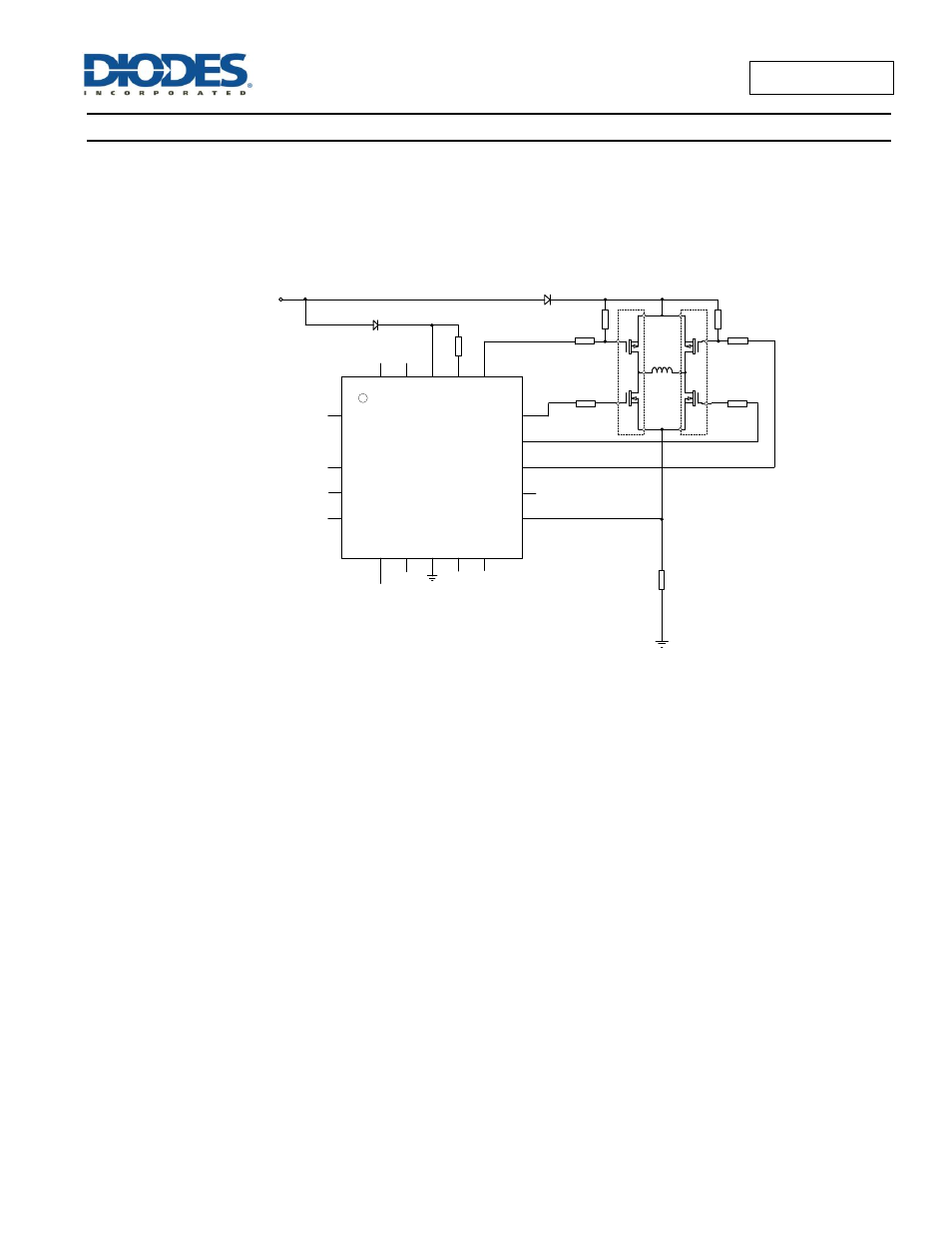
Output Device Driving
In order to drive the output stage efficiently, it is important to minimise shoot-through currents. The ZXBM1021 has a built-in delay (commutation
dead-time) to allow time for re-circulating currents to be absorbed however parasitic shoot-through can still occur. This is when the rapid switch-
on of the low-side MOSFET causes a low-going pulse through the high-side MOSFET to the gate, causing it to switch on momentarily. Slowing
the switch-on of the low-side MOSFET can eliminate this effect.
The resistors R1 to R6 and R12 in the diagram allow for control of switch-on and switch-off times for the top and bottom MOSFETs separately.
High-side MOSFETs switching speed:
R3 and R5 control the discharge of the gates of the high-side P-channel MOSFETSs, limiting the switch-on speed.
R4 and R6 control the charging of the gates of the P-channel MOSFETs, limiting the switch-off speed.
Low-side MOSFETs switching speed:
R1 and R2 are series gate resistors for the N-channel FETs, affecting both switch-on and switch-off times.
R12 is the series resistor for the V+OP pin of the ZXBM1021. This resistor is effectively in series with R1 or R2 when that
low-side N-channel device is switched on, limiting the switch-on time. R12 allows to vary the switch-on time relative to the
switch-off time to prevent parasitic shoot-through at turn-on.
When using bipolar output devices the resistors serve similar functions in limiting the base currents of the transistors.
H
+
ThRef
PWMSPD
P
h
2
H
i
H
-
SPD
F
G
Ph1Lo
Ph2Lo
Ph1Hi
SetThRef
Sense
S
e
tT
h
G
N
D
HBIAS
ZXBM1021
1
2
3
4
5
6
7
8
9
10
15
14
13
12
11
20
19
18
17
16
V
+
O
P
C
L
C
K
S
M
IN
C
SPD
V
C
C
Rsense
Motor
coil
R5
R3
R6
R4
R1
R2
R12
D2
D1
D1
Optional,
system dependent
O
p
ti
o
n
a
l
System supply
(12V)