Zxbm1021, Absolute maximum ratings, Recommended operating conditions – Diodes ZXBM1021 User Manual
Page 5: Electrical characteristics
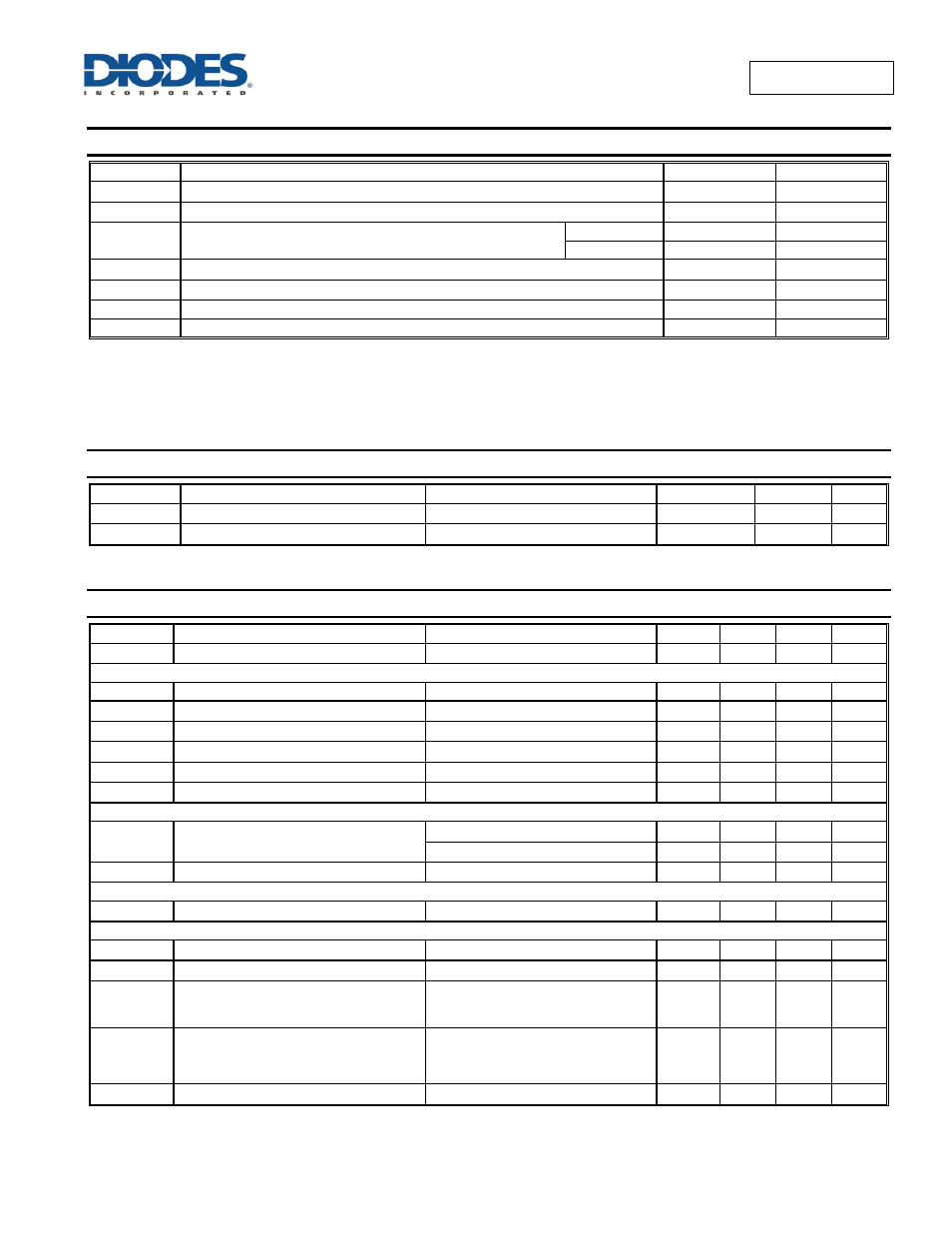
ZXBM1021
Document number: DS36322 Rev. 2 - 2
5 of 25
April 2014
© Diodes Incorporated
ZXBM1021
Absolute Maximum Ratings
(Note 6) @T
A
= +25°C, unless otherwise specified.)
Symbol
Characteristics
Values
Unit
V
CCMAX
Supply Voltage (Note 7)
-0.6 to 20
V
I
CCMAX
IC Input Current
200
mA
P
DMAX
Power Dissipation
(See thermal de-
rating curve on ‘Thermal Performance’ section)
U-QFN4040-20
820
mW
QSOP-20
820
mW
T
ST
Storage Temperature Range
-55 to +150
°C
T
J
Maximum Junction Temperature
150
°C
ESD HBM
Human Body Model (HBM) ESD Capability
2
kV
ESD MM
Machine Model (MM) ESD Protection
300
V
Notes:
6. Stresses greater than the 'Absolute Maximum Ratings' specified above may cause permanent damage to the device. These are stress ratings only;
functional operation of the device at these or any other conditions exceeding those indicated in this specification is not implied. Device reliability may be
affected by exposure to absolute maximum rating conditions for extended periods of time.
7. The absolute maximum V
CC
of 20V is a transient stress rating and is not meant as a functional operating condition. It is not recommended to operate
the device at the absolute maximum rated conditions for any period of time.
Recommended Operating Conditions
Symbol
Characteristic
Conditions
Min
Max
Unit
V
CC
Supply Voltage
Operating, -40°C to +110°C
6.8
18.0
V
T
A
Operating Temperature Range
Operating
-40
+110
°C
Electrical Characteristics
(@T
A
= +25°C, V
DD
= 12V, unless otherwise specified.)
Symbol
Characteristics
Conditions
Min
Typ
Max
Unit
I
CC
Supply Current
No Load (Note 8)
—
10
15
mA
Hall Connections
VIN
Hall Amplifier Input Voltage
Diff peak to peak
40
—
mV
V
CM
Hall Amplifier Common Mode Voltage
0.5
—
V
ThRef
V
V
HYS
Hall Amplifier Input Hysteresis
—
±12
mV
I
BS
Hall Amplifier Bias Current
—
700
1000
nA
V
HB
Hall Bias Voltage
I
HB
= 10mA
1.5
1.75
1.95
V
I
HB
Hall Bias Output Current Capability
—
—
10
mA
Reference Voltage
V
ThRef
ThRef Reference Output Voltage
I
OThRef
= 10mA, +25°C
4.85
5
5.15
V
I
OThRef
= 10mA, -40°C to +110°C
4.75
5
5.25
V
I
OThRef
ThRef Output Current Capability
—
—
10
mA
PWM Oscillator
F
PWM
PWM Frequency
18
25
—
kHz
DC Voltage Speed Control
V
SPDL
SPD Voltage Minimum
100% PWM drive
—
1
—
V
V
SPDH
SPD Voltage Maximum
0% PWM drive
—
3
—
V
I
SPD
SPD Pin Current at speed demand of 50%
of the full speed and without minimum
speed setting
V
SPD
= 2V
S
MIN
= 0V
—
0.5
2
µA
I
SPD_SMIN2V
SPD Pin Current with minimum speed
setting of 50% of the full speed
V
SPD
= 3V
R
SPD
=10k
Ω
S
MIN
= 2V
—
100
—
µA
Lin
SPD
SPD Pin voltage to output PWM linearity
V
SPD
= 2V
—
—
3
%
Note:
8. Measured with pins H+, H-, C
LCK
and C
PWM
and all other signal pins open circuit.