Zxbm1021, Pin descriptions – Diodes ZXBM1021 User Manual
Page 3
ZXBM1021
Document number: DS36322 Rev. 2 - 2
3 of 25
April 2014
© Diodes Incorporated
ZXBM1021
Pin Descriptions
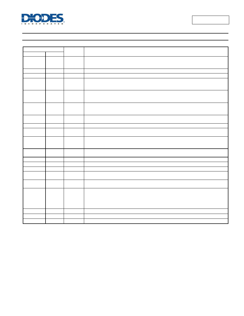
Package types: U-QFN4040-20 and QSOP-20
Pin Number
Pin
Name
Description
U-QFN4040-20 QSOP-20
1
4
HBIAS
Hall Bias Supply Voltage Output Pin. Output voltage is 1.75V typical to supply the external un-
buffered (‘naked’) Hall element. A resistance can be added in series with Hall element if lower bias
voltage is needed.
2
5
ThRef
5V Reference Voltage Output Pin. This voltage is used to supply the external networks.
3
6
PWMSPD
Speed Control PWM Signal Input Pin. PWM signal should be between 0% to 100% duty ratio.
4
7
SPD
DC Voltage Speed Control Input Pin. The control signal voltage should be between 3V for 0%
(stop) to 1V for 100% (full speed) speed control. In DC voltage mode, connect a capacitor between
SPD and ground.
5
8
C
SPD
Output Pin of the PWM Speed Control Input Signal Integrator. In PWM speed control mode,
connect a 0.1
F capacitor from C
SPD
pin to ground and connect C
SPD
pin to SPD pin. In DC
voltage speed control mode, leave this pin unconnected.
6
9
S
MIN
Minimum Speed Setting Pin. Voltage between 3V to 1V on this pin sets the minimum speed the
motor is run at between 0% to full speed. The lowest minimum speed achieved depends on the
motor coil design.
7
10
C
LCK
Rotor Lock Detect, Auto Restart Timing and Soft-Start Timing Control Pin. Typically a 470nF
capacitor is connected to this pin to set the soft-start (to full speed), lock detect and restart timings.
8
11
GND
Supply Return Ground Pin
9
12
FG
Frequency Generator Output to Provide a Tachometer Signal. This is a buffered output from the
Hall amplifier.
10
13
SetTh
Current Sense Threshold Setting Pin. Used to set the threshold voltage that represents the
maximum current to be taken by the motor. The current sense voltage at Sense pin is compared to
the SetTh voltage.
11
14
Sense
Current Sense Pin. Input for the signal from a sense resistor in the ground return of the H-bridge
circuit to represent the current taken by the motor.
12
15
SetThRef
A variable voltage source used to set the voltage on the SetTh pin.
13
16
Ph1Hi
Phase 1 High-Side External Power Switch Drive Output Pin. This is a 50mA open-collector output.
14
17
Ph2Hi
Phase 2 High-Side External Power Switch Drive Output Pin. This is a 50mA open-collector output.
15
18
Ph2Lo
Phase-2 Low-Side External Power Switch Drive Output Pin. Darlington emitter follower output with
active pull down to give source/sink current of 100mA/100mA.
16
19
Ph1Lo
Phase-1 Low-Side External Power Switch Drive Output Pin. Darlington emitter follower output with
active pull down to give source/sink current of 100mA/100mA.
17
20
V+OP
Phase Low Output Supply Pin. Only the low side output drives for Ph1Lo and Ph2Lo are supplied
by the V+OP pin. For external MOSFET power devices, a resistor from V
CC
pin to V+OP slows
down the turn-on speed of the low-side MOSFET S and therefore helps prevent shoot-through
during turn-on of low-side switches. For external Bipolar power devices, a resistor between the
V
CC
pin and V+OP controls the current into the transistor base.
18
1
V
CC
Power Supply Pin
19
2
H+
Hall Device Positive Input Pin. When H+ is higher in relation to H-, Ph2 is active.
20
3
H-
Hall Device Negative Input Pin