Diodes SBL2030CT - SBL2060CT User Manual
Features, Mechanical data, Maximum ratings and electrical characteristics
DS23015 Rev. 9 - 2
1 of 3
www.diodes.com
SBL2030CT - SBL2060CT
© Diodes Incorporated
SBL2030CT - SBL2060CT
20A SCHOTTKY BARRIER RECTIFIER
Features
• Schottky
Barrier
Chip
•
Guard Ring Die Construction for Transient Protection
•
Low Power Loss, High Efficiency
•
High Surge Capability
•
High Current Capability and Low Forward Voltage Drop
•
For Use in Low Voltage, High Frequency Inverters, Free
Wheeling, and Polarity Protection Applications
•
Lead Free Finish, RoHS Compliant (Note 3)
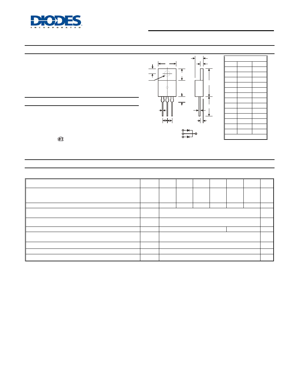
Mechanical Data
• Case:
TO-220AB
•
Case Material: Molded Plastic. UL Flammability
Classification Rating 94V-0
•
Moisture Sensitivity: Level 1 per J-STD-020D
•
Polarity: As Marked on Body
•
Terminals: Finish – Tin. Solderable per MIL-STD-202,
Method 208
•
Marking: Type Number
•
Weight: 2.24 grams (approximate)
L
M
A
N
P
D
E
K
C
B
G
1
2
3
J
H H
Pin 1 +
Pin 3 +
Pin 2 -
Case
+
TO-220AB
Dim
Min
Max
A
14.48
15.75
B
10.00
10.40
C
2.54
3.43
D
5.90
6.40
E
2.80
3.93
G
12.70
14.27
H
2.40
2.70
J
0.69
0.93
K
3.54
3.78
L
4.07
4.82
M
1.15
1.39
N
0.30
0.50
P
2.04
2.79
All Dimensions in mm
Maximum Ratings and Electrical Characteristics
@T
A
= 25°C unless otherwise specified
Single phase, half wave, 60 Hz, resistive or inductive load.
For capacitive load, derate current by 20%.
Characteristic
Symbol
SBL
2030CT
SBL
2035CT
SBL
2040CT
SBL
2045CT
SBL
2050CT
SBL
2060CT
Unit
Peak Repetitive Reverse Voltage
Working Peak Reverse Voltage
DC Blocking Voltage
V
RRM
V
RWM
V
R
30
35
40
45
50
60
V
RMS Reverse Voltage
V
R(RMS)
21
24.5
28
31.5
35
42
V
Average Rectified Output Current
(Note 1)
@ T
C
= 95
°C
I
O
20
A
Non-Repetitive Peak Forward Surge Current 8.3ms
Single Half Sine-Wave Superimposed on Rated Load
I
FSM
250
A
Forward Voltage Drop
@ I
F
= 10A, T
C
= 25
°C
V
FM
0.55
0.75
V
Peak Reverse Current
@ T
C
= 25
°C
at Rated DC Blocking Voltage
@ T
C
= 100
°C
I
RM
1.0
50
mA
Typical Junction Capacitance (Note 2)
C
j
650
pF
Typical Thermal Resistance Junction to Case (Note 1)
R
θJC
2.8
°C/W
Operating and Storage Temperature Range
T
J,
T
STG
-65 to +150
°C
Notes:
1. Thermal resistance junction to case mounted on heatsink.
2. Measured at 1.0MHz and applied reverse voltage of 4.0V DC.
3. EU Directive 2002/95/EC (RoHS). All applicable RoHS exemptions applied, see