Max3301e usb on-the-go transceiver and charge pump, Pin description – Rainbow Electronics MAX3301E User Manual
Page 9
MAX3301E
USB On-the-Go Transceiver and Charge Pump
_______________________________________________________________________________________
9
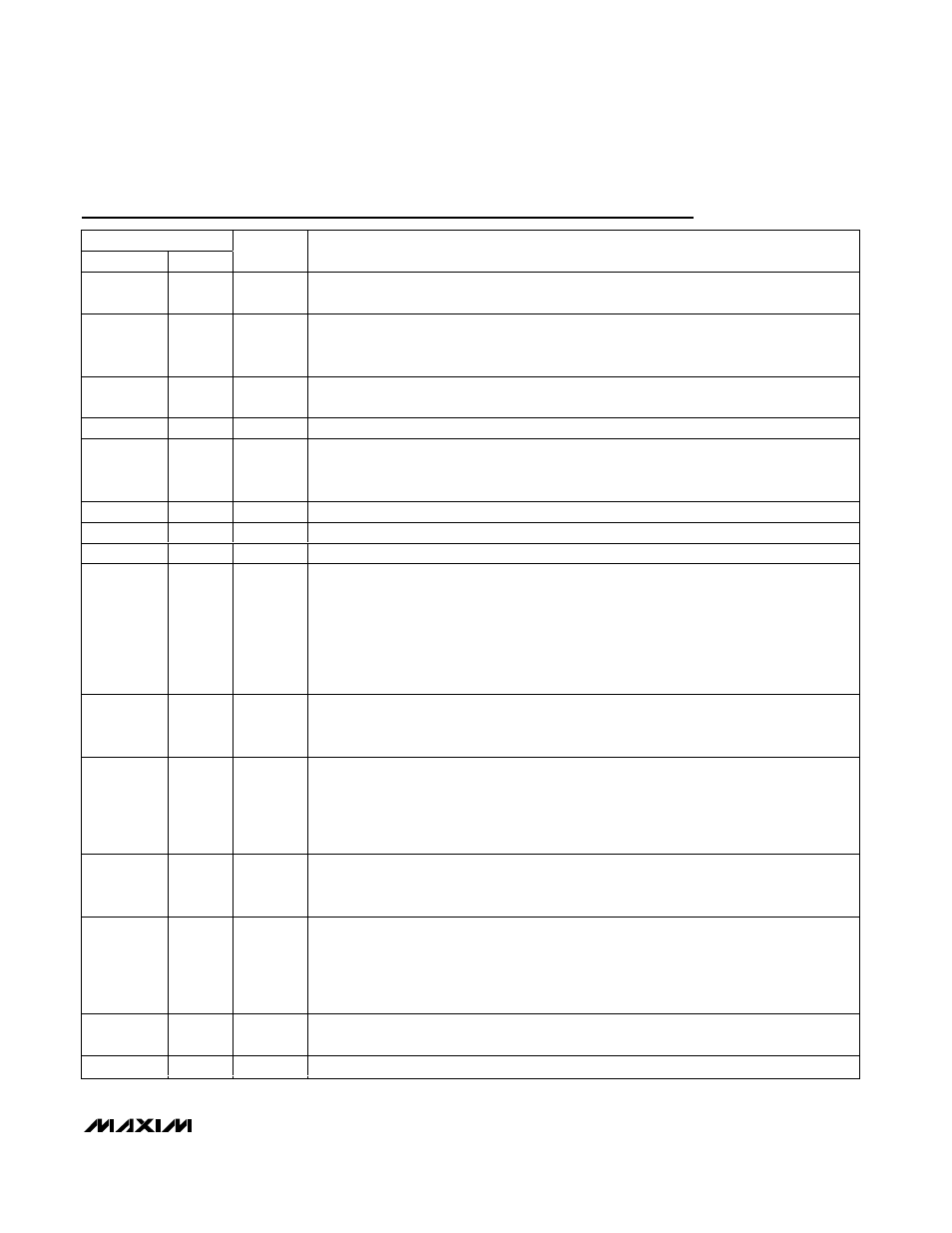
Pin Description
PIN
THIN QFN
UCSP
NAME
FUNCTION
1, 4, 9, 12,
17, 25, 28
—
N.C.
No Connection. Not internally connected.
2
D2
DAT_VP
System-Side Data Input/Output. DAT_VP is an input if OE/INT is logic 0. DAT_VP is an output
if OE/INT is logic 1. Program the function of DAT_VP with the dat_se0 bit (bit 2 of control
register 1, see Table 7).
3, 29
D1, E3
V
CC
Input Power Supply. Connect a +3V to +4.5V supply to V
CC
and bypass to GND with a 1µF
capacitor. The supply range enables direct powering from one Li+ battery.
5
C1
C-
Charge-Pump Flying-Capacitor Negative Terminal
6
C2
SE0_VM
System-Side Data Input/Output. SE0_VM is an input if OE/INT is logic 0. SE0_VM is an output
if OE/INT is logic 1. Program the function of SE0_VM with the dat_se0 bit (bit 2 of control
register 1, see Table 7).
7, 21
B1, C5
GND
Ground
8
A1
SDA
I
2
C-Compatible Serial Data Interface. Open-drain data input/output.
10
B2
SCL
I
2
C-Compatible Serial Clock Input
11
A2
OE/INT
O utp ut E nab l e. O E/INT contr ol s the i np ut or outp ut status of D AT_V P /S E 0_V M and D + /D - . When
O E/INT i s l og i c 0, the d evi ce i s i n tr ansm i t m od e. W hen O E/INT i s l og i c 1, the d evi ce i s i n
r ecei ve m od e. W hen i n susp end m od e, O E/INT can b e p r og r am m ed to functi on as an i nter r up t
outp ut that d etects the sam e i nter r up ts as INT. The oe_i nt_en b i t ( b i t 5 of contr ol r eg i ster 1, see
Tab l e 7) enab l es and d i sab l es the i nter r up t ci r cui tr y of O E/INT. The i r q _m od e b i t ( b i t 1 of
sp eci al - functi on r eg i ster 1, see Tab l e 14) p r og r am s the outp ut confi g ur ati on of INT and O E/INT
as op en- d r ai n or p ush- p ul l .
13
A3
RCV
D+ and D- Differential Receiver Output. In receive mode (see Table 4), when D+ is high and
D- is low, RCV is high. In receive mode, when D+ is low and D- is high, RCV is low. RCV is
low in suspend mode.
14
B3
SPD
Speed-Selector Input. Connect SPD to GND to select the low-speed data rate (1.5Mbps).
Connect SPD to V
L
to select the full-speed data rate (12Mbps). Disable the SPD input by
writing a 1 to spd_susp_ctl (bit 1 in special-function register 1, see Table 14). The speed bit
(bit 0 of control register 1, see Table 7) determines the maximum data rate of the MAX3301E
when the SPD input is disabled.
15
A4
V
L
System-Side Logic-Supply Input. Connect to the system’s logic-level power supply, +1.65V
to +3.6V. This sets the maximum output levels of the logic outputs and the input thresholds of
the logic inputs. Bypass to GND with a 0.1µF capacitor.
16
A5
SUS
Active-High Suspend Input. Drive SUS low for normal USB operation. Drive SUS high to
enable suspend mode. RCV asserts low in suspend mode. Disable the SUS input by writing
a 1 to spd_susp_ctl (bit 1 in special-function register 1, see Table 14). The suspend bit (bit 1
of control register 1, see Table 7) determines the operating mode of the MAX3301E when the
SUS input is disabled.
18
B4
INT
Active-Low Interrupt Source. Program the INT output as push-pull or open-drain with the
irq_mode bit (bit 1 of special-function register 2, see Table 15).
19
B5
RESET
Active-Low Reset Input. Drive RESET low to asynchronously reset the MAX3301E.