Max3301e usb on-the-go transceiver and charge pump, Pin description (continued), Test circuits and timing diagrams – Rainbow Electronics MAX3301E User Manual
Page 10
MAX3301E
USB On-the-Go Transceiver and Charge Pump
10
______________________________________________________________________________________
Pin Description (continued)
PIN
THIN QFN
UCSP
NAME
FUNCTION
20
C3
ADD
I
2
C-Interface Address Selection Input. (See Table 5.)
22
C4
ID_IN
ID Input. ID_IN is internally pulled up to V
CC
. The state of ID_IN determines ID bits 3 and 5 of
the interrupt source register (see Table 10).
23
D5
D-
USB Differential Data Input/Output. Connect D- to the D- terminal of the USB connector
through a 27.4
Ω ±1% series resistor.
24
E5
D+
USB Differential Data Input/Output. Connect D+ to the D+ terminal of the USB connector
through a 27.4
Ω ±1% series resistor.
26
D4
VM
Single-Ended Receiver Output. VM functions as a receiver output in all operating modes. VM
duplicates D-.
27
E4
TRM
USB Transceiver Regulated Output Voltage. TRM provides a regulated 3.3V output. Bypass
TRM to GND with a 1µF ceramic capacitor installed as close to the device as possible. TRM
normally derives power from V
CC
. TRM provides power to internal circuitry and provides the
pullup voltage for the internal USB pullup resistor. Do not use TRM to power external
circuitry. The reg_sel bit (bit 3 of special-function register 2, see Table 15) controls the TRM
power source with software.
30
D3
VP
Single-Ended Receiver Output. VP functions as a receiver output in all operating modes. VP
duplicates D+.
31
E2
V
BUS
USB Bus Power. Use V
BUS
as an output to power the USB bus, or as an input to power the
internal linear regulator. Bits 5 to 7 of control register 2 (see Table 8) control the charging
and discharging functions of V
BUS
.
32
E1
C+
Charge-Pump Flying-Capacitor Positive Terminal
EP
—
EP
Exposed Paddle. Connect to GND or leave floating
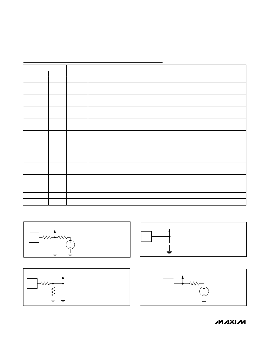
Test Circuits and Timing Diagrams
DUT
27.4
Ω
220
Ω
TEST POINT
C
L
V
D+/D-
LOAD FOR DISABLE TIME (D+/D-) MEASUREMENT
V = 0 FOR t
PHZ
V = V
TRM
FOR t
PLZ
C
L
= 50pF FOR FULL SPEED,
C
L
= 200pF TO 600pF FOR LOW SPEED
Figure 1. Load for Disable Time Measurement
DUT
27.4
Ω
15k
Ω
TEST POINT
C
L
D+/D-
LOAD FOR
1) ENABLE TIME (D+/D-) MEASUREMENT
2) DAT_VP/SEO_VM TO D+/D- PROPAGATION DELAY
3) D+/D- RISE/FALL TIMES
C
L
= 50pF FOR FULL SPEED,
C
L
= 200pF TO 600pF FOR LOW SPEED
Figure 2. Load for Enable Time, Transmitter Propagation Delay,
and Transmitter Rise/Fall Times
DUT
TEST POINT
C
L
RCV, VP, VM,
DAT_VP,
SEO_VM
LOAD FOR
1) D+/D- TO RCV/VP/VM/DAT_VP/SEO_VM PROPAGATION DELAYS
2) RCV/VP/VM/DAT_VP/SEO_VM RISE/FALL TIMES (C
L
= 15pF)
Figure 3. Load for Receiver Propagation Delay and Receiver
Rise/Fall Times
DUT
270
Ω
TEST POINT
V = 2/3 x V
L
DAT_VP
SEO_VM
Figure 4. Load for DAT_VP, SE0_VM Enable/Disable Time
Measurements