Max3301e usb on-the-go transceiver and charge pump, Table 16. id registers – Rainbow Electronics MAX3301E User Manual
Page 27
MAX3301E
USB On-the-Go Transceiver and Charge Pump
______________________________________________________________________________________
27
ID and Manufacturer Register Address Map
Table 16 provides the contents of the ID registers of the
MAX3301E. Addresses 00h and 01h comprise the ven-
dor ID registers. Addresses 02h and 03h comprise the
product ID registers. Addresses 14h and 15h comprise
the revision ID registers.
Audio Car Kit
Many cell phones are required to interface to car kits.
Depending upon the car kit, the interface to the phone
may be required to support any or all of the following
functions:
•
Audio input
•
Audio output
•
Charging
•
Control and status
D+ and D- of the MAX3301E go to a high-impedance
state when in shutdown mode, allowing external signals
(including audio) to be multiplexed onto these lines.
External Components
External Resistors
Two external resistors (27.4
Ω ±1%) are required for
USB connection. Install one resistor in series between
D+ of the MAX3301E and D+ of the USB connector.
Install the other resistor in series between D- of the
MAX3301E and D- of the USB connector (see the
Typical Operating Circuit).
External Capacitors
Five external capacitors are recommended for proper
operation. Install all capacitors as close to the device as
possible. Decouple V
L
to GND with a 0.1µF ceramic
capacitor. Bypass V
CC
to GND with a 1µF ceramic
capacitor. Bypass TRM to GND with a 1µF (or greater)
ceramic or plastic capacitor. Connect a 100nF flying
capacitor between C+ and C- for the charge pump (see
the Typical Operating Circuit). Bypass V
BUS
to GND
with a 1µF to 6.5µF ceramic capacitor in accordance
with USB OTG specifications.
ESD Protection
To protect the MAX3301E against ESD, D+, D-, ID_IN,
and V
BUS
have extra protection against static electricity
to protect the device up to ±15kV. The ESD structures
withstand high ESD in all states; normal operation, sus-
pend mode, interrupt shutdown, and shutdown. For the
ESD structures to work correctly, connect a 1µF or
greater capacitor from TRM to GND and from V
BUS
to
GND. ESD protection can be tested in various ways; the
D+, D-, ID_IN, and V
BUS
inputs/outputs are character-
ized for protection to the following limits:
•
±15kV using the Human Body Model
•
±6kV using the IEC 61000-4-2 Contact Discharge
Method
•
±10kV using the IEC 61000-4-2 Air-Gap Discharge
Method
REGISTER
ADDRESS
CONTENTS
00h
6Ah
Vendor ID
01h
0Bh
02h
01h
Product ID
03h
33h
14h
77h
Revision ID
15h
41h
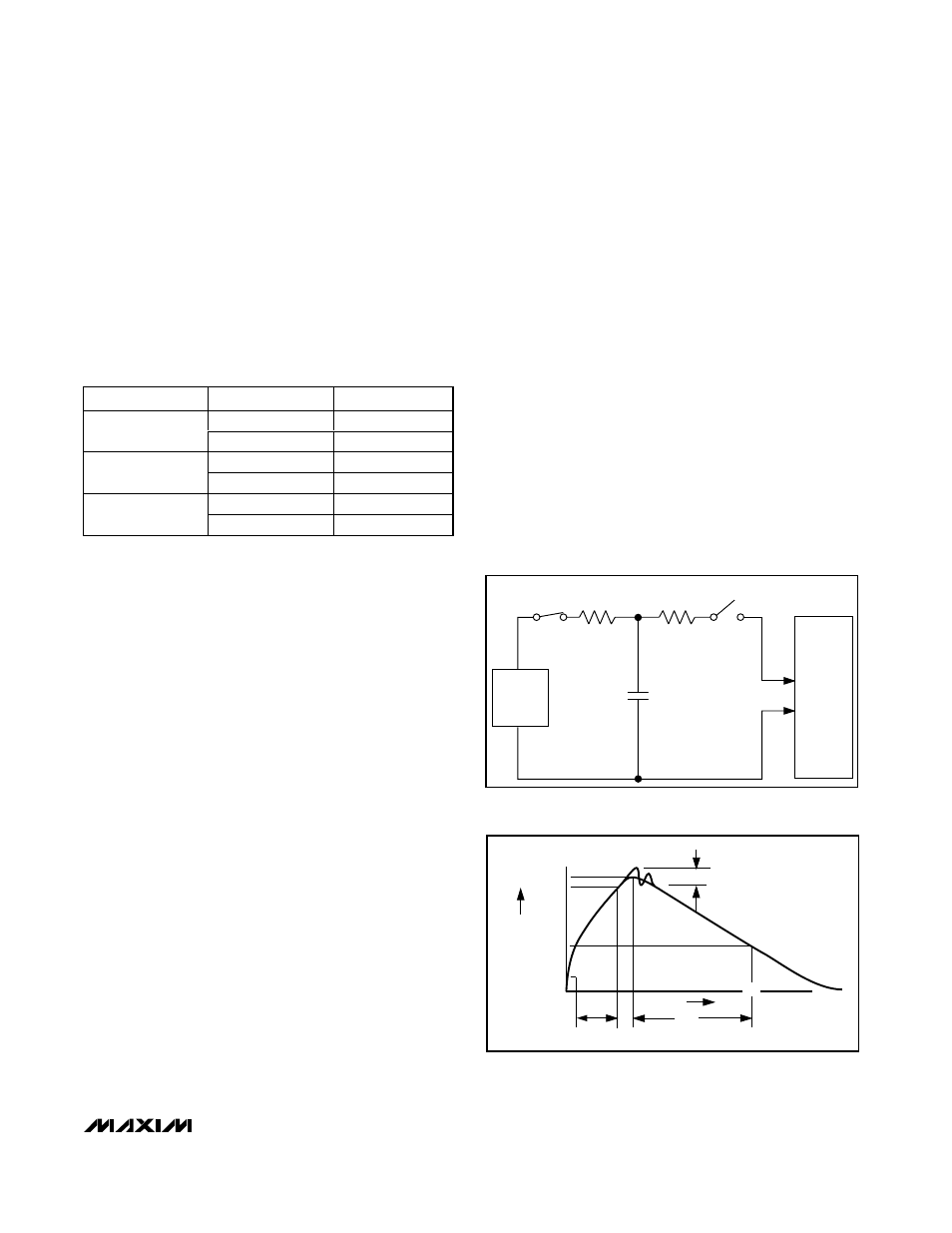
Table 16. ID Registers
CHARGE-CURRENT-
LIMIT RESISTOR
DISCHARGE
RESISTANCE
STORAGE
CAPACITOR
Cs
100pF
R
C
1M
Ω
R
D
1500
Ω
HIGH-
VOLTAGE
DC
SOURCE
DEVICE
UNDER
TEST
Figure 22. Human Body ESD Test Modes
I
P
100%
90%
36.8%
t
RL
TIME
t
DL
CURRENT WAVEFORM
PEAK-TO-PEAK RINGING
(NOT DRAWN TO SCALE)
Ir
10%
0
0
AMPERES
Figure 23. Human Body Model Current Waveform