Max3301e usb on-the-go transceiver and charge pump, Detailed description – Rainbow Electronics MAX3301E User Manual
Page 13
MAX3301E
USB On-the-Go Transceiver and Charge Pump
______________________________________________________________________________________
13
Detailed Description
The USB OTG specification defines a dual-role USB
device that acts either as an A device or as a B device.
The A device supplies power on V
BUS
and initially
serves as the USB host. The B device serves as the ini-
tial peripheral and requires circuitry to monitor and pulse
V
BUS
. These initial roles can be reversed using HNP.
The MAX3301E combines a low- and full-speed USB
transceiver with additional circuitry required by a dual-
role device. The MAX3301E employs flexible switching
circuitry to enable the device to act as a dedicated host
or peripheral USB transceiver. For example, the charge
pump can be turned off and the internal regulator can
be powered from V
BUS
for bus-powered peripheral
applications.
Transceiver
The MAX3301E transceiver complies with the USB ver-
sion 2.0 specification, and operates at full-speed
(12Mbps) and low-speed (1.5Mbps) data rates. Set the
data rate with the SPD input. Set the direction of data
transfer with the OE/INT input. Alternatively, control trans-
ceiver operation with control register 1 (Table 7) and spe-
cial-function registers 1 and 2 (see Tables 14 and 15).
Level Shifters
Internal level shifters allow the system-side interface to
run at logic-supply voltages as low as +1.65V. Interface
logic signals are referenced to the voltage applied to
the logic-supply voltage, V
L
.
Charge Pump
The MAX3301E’s OTG-compliant charge pump oper-
ates with +3V to +4.5V input supply voltages (V
CC
) and
supplies a +4.8V to +5.25V OTG-compatible output on
V
BUS
while sourcing the 8mA or greater output current
that an A device is required to supply. Connect a 0.1µF
flying capacitor between C+ and C-. Bypass V
BUS
to
GND with a 1µF to 6.5µF capacitor, in accordance with
USB OTG specifications. The charge pump can be
turned off to conserve power when not used. Control of
the charge pump is set through the vbus_drv bit (bit 5)
of control register 2 (see Table 8).
Linear Regulator (TRM)
An internal 3.3V linear regulator powers the transceiver
and the internal 1.5k
Ω D+/D- pullup resistor. Under the
control of internal register bits, the linear regulator can
be powered from V
CC
or V
BUS
. The regulator power-
supply settings are controlled by the reg_sel bit (bit 3) in
special-function register 2 (see Table 15). This flexibility
allows the system designer to configure the MAX3301E
for virtually any USB power situation.
The output of the TRM is not a power supply. Do not use
as a power source for any external circuitry. Connect a
1.0µF (or greater) ceramic or plastic capacitor from TRM
to GND, as close to the device as possible.
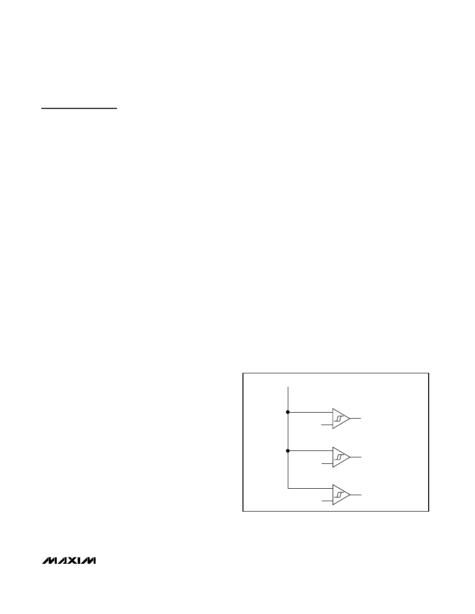
V
BUS
Level-Detection Comparators
Comparators drive interrupt source register bits 0, 1,
and 7 (Table 10) to indicate important USB OTG V
BUS
voltage levels:
•
V
BUS
is valid (vbus_vld)
•
USB session is valid (sess_vld)
•
USB session has ended (sess_end)
The vbus_valid comparator sets vbus_vld to 1 if V
BUS
is
higher than the V
BUS
valid comparator threshold. The
V
BUS
valid status bit (vbus_vld) is used by the A device
to determine if the B device is sinking too much current
(i.e., is not supported). The session_valid comparator
sets sess_vld to 1 if V
BUS
is higher than the session
valid comparator threshold. This status bit indicates that
a data transfer session is valid. The session_end com-
parator sets sess_end to 1 if V
BUS
is higher than the
session end comparator threshold. Figure 12 shows the
level-detector comparators. The interrupt-enable regis-
ters (Tables 12 and 13) determine whether a falling or
rising edge of V
BUS
asserts these status bits.
Figure 12. Comparator Network Diagram
V
BUS
VBUS_VLD
V
TH-VBUS
V
TH-SESS_VLD
V
TH-SESS_END
SESS_VLD
SESS_END