Max3301e usb on-the-go transceiver and charge pump – Rainbow Electronics MAX3301E User Manual
Page 19
MAX3301E
USB On-the-Go Transceiver and Charge Pump
______________________________________________________________________________________
19
Acknowledge
The acknowledge bit (ACK) is the 9th bit attached to
any 8-bit data word. ACK is always generated by the
receiving device. The MAX3301E generates an ACK
when receiving an address or data by pulling SDA low
during the ninth clock period. When transmitting data,
the MAX3301E waits for the receiving device to gener-
ate an ACK. Monitoring ACK allows for detection of
unsuccessful data transfers. An unsuccessful data
transfer occurs if a receiving device is busy or if a sys-
tem fault has occurred. In the event of an unsuccessful
data transfer, the bus master should reattempt commu-
nication at a later time.
Slave Address
A bus master initiates communication with a slave
device by issuing a START condition followed by the 7-
bit slave address (see Figure 15). When idle, the
MAX3301E waits for a START condition followed by its
slave address. The LSB of the address word is the
read/write (R/W) bit. R/W indicates whether the master
is writing to or reading from the MAX3301E (R/W = 0
selects the write condition, R/W = 1 selects the read
condition). After receiving the proper address, the
MAX3301E issues an ACK.
The MAX3301E has two possible addresses (see Table
5). Address bits A6 through A1 are preset, while a reset
condition or an I
2
C general call address loads the value
of A0 from ADD. Connect ADD to GND to set A0 to 0.
Connect ADD to V
L
to set A0 to 1. This allows up to two
MAX3301Es to share the same bus.
Write Byte Format
Writing data to the MAX3301E requires the transmission
of at least 3 bytes. The first byte consists of the
MAX3301E’s 7-bit slave address, followed by a 0 (R/W
bit). The second byte determines which register is to be
written to. The third byte is the new data for the selected
register. Subsequent bytes are data for sequential reg-
isters. Figure 18 shows the typical write byte format.
Read Byte Format
Reading data from the MAX3301E requires the trans-
mission of at least 3 bytes. The first byte consists of the
MAX3301E’s slave address, followed by a zero (R/W
bit). The second byte selects the register from which
data is read. The third byte consists of the MAX3301’s
slave address, followed by a one (R/W bit). The master
then reads one or more bytes of data. Figure 19 shows
the typical read byte format.
Burst-Mode Write Byte Format
The MAX3301E allows a master device to write to
sequential registers without repeatedly sending the
slave address and register address each time. The
master first sends the slave address, followed by a zero
to write data to the MAX3301E. The MAX3301E sends
an acknowledge bit back to the master. The master
sends the 8-bit register address and the MAX3301E
returns an acknowledge bit. The master writes a data
byte to the selected register and receives an acknowl-
edge bit if a supported register address has been cho-
sen. The register address increments and is ready for
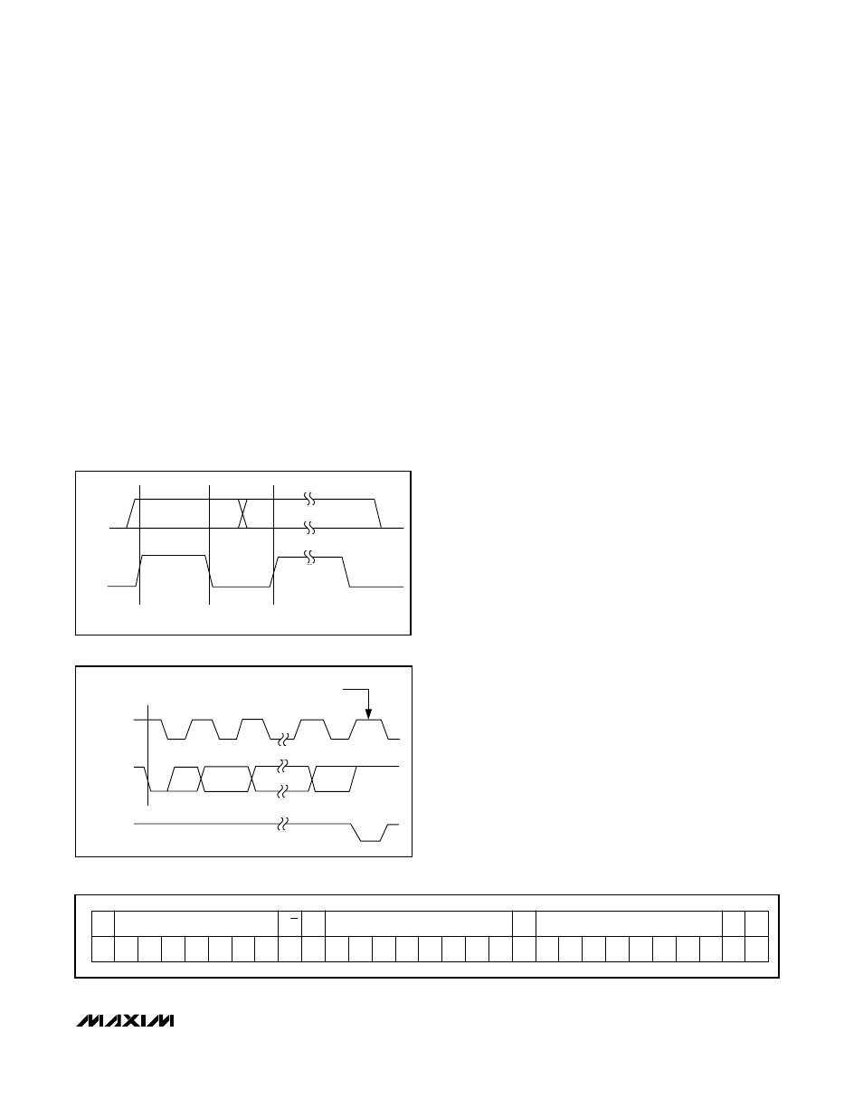
SDA
SCL
DATA LINE STABLE,
DATA VALID
CHANGE OF DATA
ALLOWED
Figure 16. Bit Transfer
SCL
START
CONDITION
S
SDA BY
TRANSMITTER
SDA BY
RECEIVER
CLOCK PULSE FOR ACKNOWLEDGEMENT
1
2
8
9
Figure 17. Acknowledge
A
REGISTER ADDRESS
(8 BITS)
MSB
LSB
A
A
P
MSB
LSB
DATA
(8 BITS)
S
SLAVE ADDRESS
(7 BITS)
A6
A5
A4
A3
A2
A1
A0
0
R/W
Figure 18. Write-Byte Format