Max3301e usb on-the-go transceiver and charge pump – Rainbow Electronics MAX3301E User Manual
Page 16
MAX3301E
USB On-the-Go Transceiver and Charge Pump
16
______________________________________________________________________________________
General-Purpose Buffer Mode
Set gp_en (bit 7 in special-function register 1) and
dat_se0 (bit 2 in control register 1) to 1, set uart_en (bit 6
in control register 1) to zero, and drive OE/INT low to
place the MAX3301E in general-purpose buffer mode.
Control the direction of data transfer with dminus_dir and
dplus_dir (bits 3 and 4 of special-function register 1, see
Tables 2 and 14).
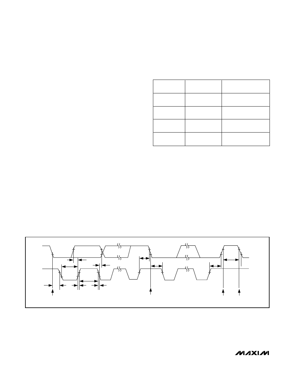
Serial Addressing
The MAX3301E operates as a slave device that sends
and receives control and status signals through an I
2
C-
compatible 2-wire interface. The interface uses a serial
data line (SDA) and a serial clock line (SCL) to achieve
bidirectional communication between master(s) and
slave(s). A master (typically a microcontroller) initiates
all data transfers to and from the MAX3301E and gener-
ates the SCL clock that synchronizes the data transfer
(Figure 13).
The MAX3301E SDA line operates as both an input and
as an open-drain output. SDA requires a pullup resistor,
typically 4.7k
Ω. The MAX3301E SCL line only operates
as an input. SCL requires a pullup resistor if there are
multiple masters on the 2-wire interface, or if the master
in a single-master system has an open-drain SCL output.
Each transmission consists of a start condition (see
Figure 14) sent by a master device, the MAX3301E 7-bit
slave address (determined by the state of ADD), plus an
R/W bit (see Figure 15), a register address byte, one or
more data bytes, and a stop condition (see Figure 14).
Start and Stop Conditions
Both SCL and SDA assert high when the interface is not
busy. A master device signals the beginning of a trans-
mission with a start (S) condition by transitioning SDA
from high to low while SCL is high. The master issues a
stop (P) condition by transitioning SDA from low to high
while SCL is high. The bus is then free for another trans-
mission (see Figure 14).
Bit Transfer
One data bit is transferred during each clock pulse. The
data on SDA must remain stable while SCL is high (see
Figure 16).
dplus_dir
dminus_ dir
DIRECTION OF DATA
TRANSFER
0
0
DAT_VP
→ D+
SE0_VM
→ D-
0
1
DAT_VP
→ D+
SE0_VM
← D-
1
0
DAT_VP
← D+
SE0_VM
→ D-
1
1
DAT_VP
← D+
SE0_VM
← D-
Table 2. Setting the Direction of Data
Transfer in General-Purpose Buffer Mode
SDA
SCL
t
HD: STA
t
SU: DAT
t
HD: DAT
t
SU: STA
t
HD: STA
t
SU: STO
t
BUF
t
LOW
t
HIGH
t
R
t
F
START
CONDITION
REPEATED START
CONDITION
STOP
CONDITION
START
CONDITION
Figure 13. 2-Wire Serial Interface Timing Details