Max3301e usb on-the-go transceiver and charge pump – Rainbow Electronics MAX3301E User Manual
Page 2

MAX3301E
USB On-the-Go Transceiver and Charge Pump
2
_______________________________________________________________________________________
ABSOLUTE MAXIMUM RATINGS
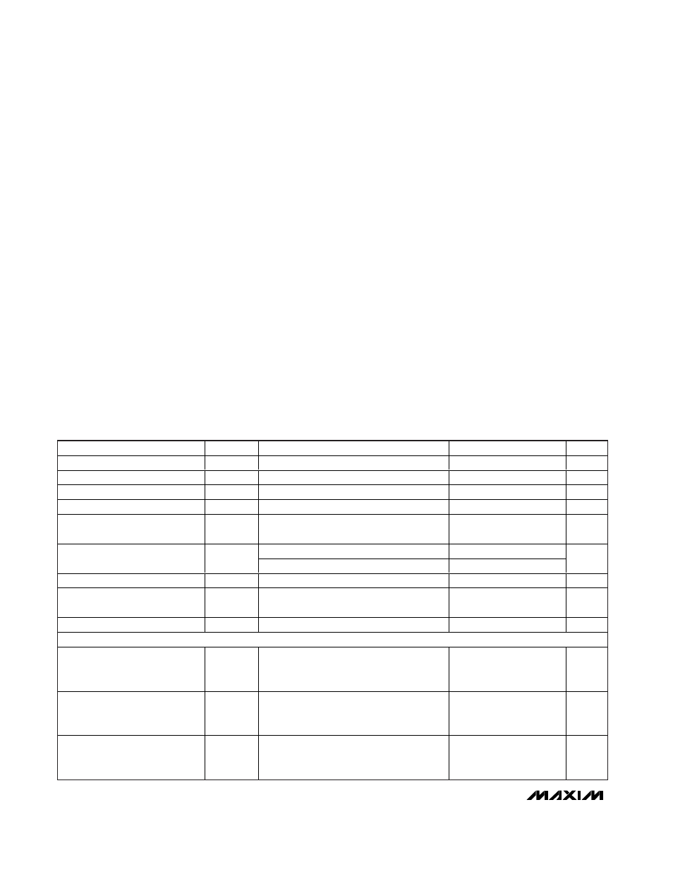
DC ELECTRICAL CHARACTERISTICS
(V
CC
= +3V to +4.5V, V
L
= +1.65V to +3.6V, C
FLYING
= 100nF, C
VBUS
= 1µF, ESR
CVBUS
= 0.1
Ω (max), T
A
= T
MIN
to T
MAX
, unless
otherwise noted. Typical values are at V
CC
= +3.7V, V
L
= +2.5V, T
A
= +25°C.) (Note 2)
Note 1: The UCSP package is constructed using a unique set of packaging techniques that impose a limit on the thermal profile the
device can be exposed to during board-level solder attach and rework. This limit permits only the use of the solder profiles recom-
mended in the industry-standard specification, JEDEC 020A, paragraph 7.6, Table 3 for IR/VPR and convection reflow. Preheating is
required. Hand or wave soldering is not allowed.
Stresses beyond those listed under “Absolute Maximum Ratings” may cause permanent damage to the device. These are stress ratings only, and functional
operation of the device at these or any other conditions beyond those indicated in the operational sections of the specifications is not implied. Exposure to
absolute maximum rating conditions for extended periods may affect device reliability.
All voltages are referenced to GND.
V
CC
, V
L
.....................................................................-0.3V to +6V
TRM (regulator off or supplied by V
BUS
) ..-0.3V to (V
BUS
+ 0.3V)
TRM (regulator supplied by V
CC
)...............-0.3V to (V
CC
+ 0.3V)
D+, D- (transmitter tri-stated) ...................................-0.3V to +6V
D+, D- (transmitter functional)....................-0.3V to (V
CC
+ 0.3V)
V
BUS
.........................................................................-0.3V to +6V
ID_IN, SCL, SDA.......................................................-0.3V to +6V
INT, SPD, RESET, ADD, OE/INT, RCV, VP,
VM, SUS, DAT_VP, SE0_VM ......................-0.3V to (V
L
+ 0.3V)
C+.............................................................-0.3V to (V
BUS
+ 0.3V)
C-................................................................-0.3V to (V
CC
+ 0.3V)
Short-Circuit Duration, V
BUS
to GND .........................Continuous
Continuous Power Dissipation (T
A
= +70°C)
5 x 5 UCSP (derate 12.2mW/°C above +70°C) ...........976mW
32-Pin Thin QFN (5mm x 5mm x 0.8mm) (derate 21.3mW/°C
above +70°C).............................................................1702mW
Operating Temperature Range ...........................-40°C to +85°C
Junction Temperature ......................................................+150°C
Storage Temperature Range .............................-65°C to +150°C
Lead Temperature (soldering, 10s) .................................+300°C
Bump Reflow Temperature (Note 1)
Infrared (15s) ...............................................................+200°C
Vapor Phase (20s) .......................................................+215°C
PARAMETER
SYM B O L
CONDITIONS
MIN
TYP
MAX
UNITS
Supply Voltage
V
CC
3.0
4.5
V
TRM Output Voltage
V
TRM
3.0
3.6
V
Logic Supply Voltage
V
L
1.65
3.60
V
V
L
Supply Current
I
VL
I
2
C interface in steady state
5
µA
V
CC
Operating Supply Current
I
CC
USB normal mode, C
L
= 50pF, device
switching at full speed
10
mA
vbus_drv = 1, I
VBUS
= 0
1.4
2
V
CC
Supply Current During Full-
Speed Idle
vbus_drv = 0, D+ = high, D- = low
0.5
0.8
mA
V
CC
Shutdown Supply Current
I
CC(SHDN)
3.5
10
µA
V
CC
Interrupt Shutdown Supply
Current
I
CC(ISHDN)
ID_IN floating or high
20
30
µA
V
CC
Suspend Supply Current
USB suspend mode, ID_IN floating or high
170
500
µA
LOGIC I/O
RC V , D AT_V P , S E 0_V M , INT,
OE/INT, V P , V M Outp ut H i g h
V ol tag e
V
OH
I
OUT
= 1mA (sourcing)
V
L
- 0.4
V
RCV, DAT_VP, SE0_VM, INT,
OE/INT, VP, VM Output Low
Voltage
V
OL
I
OUT
= 1mA (sinking)
0.4
V
OE/INT, SPD, SUS, RESET,
DAT_VP, SE0_VM Input High
Voltage
V
IH
2/3 x V
L
V
