8 programming interface timing – Rainbow Electronics AT89LP216 User Manual
Page 72

72
3621A–MICRO–6/06
AT89LP216 [Preliminary]
23.8
Programming Interface Timing
This section details general system timing sequences and constraints for entering or exiting In-
System Programming as well as parameters related to the Serial Peripheral Interface during
ISP. The general timing parameters for the following waveform figures are listed in section
23.8.1
Power-up Sequence
Execute this sequence to enter programming mode immediately after power-up. In the RST pin
is disabled or if the ISP Fuse is disabled, this is the only method to enter programming (see
).
1.
Apply power between VCC and GND pins. RST should remain low.
2.
Wait at least t
PWRUP
. and drive SS high.
3.
Wait at least t
SUT
for the internal Power-on Reset to complete. The value of t
SUT
will
depend on the current settings of the device.
4.
Start programming session.
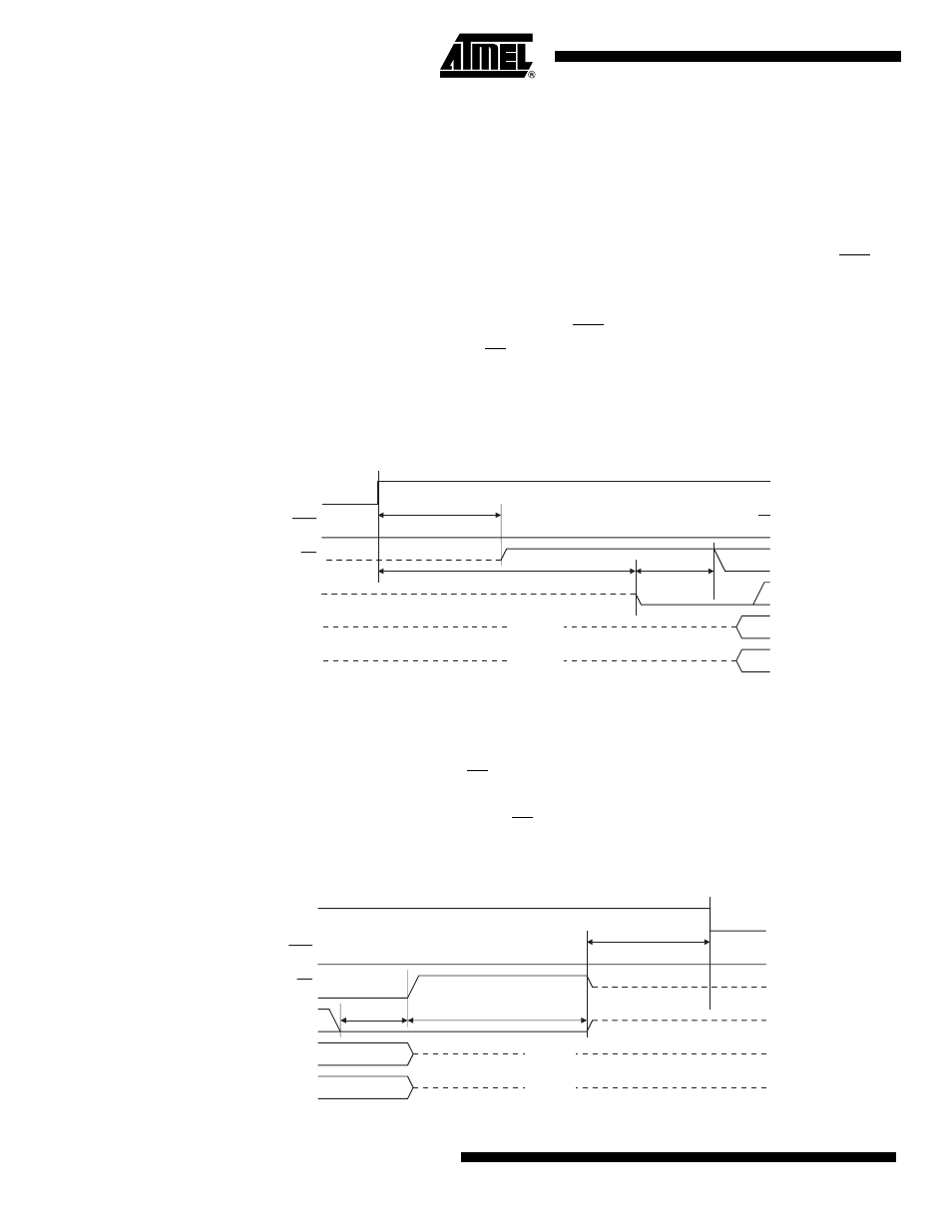
Figure 23-5. Serial Programming Power-up Sequence
23.8.2
Power-down Sequence
Execute this sequence to power-down the device after programming.
1.
Drive SCK low.
2.
Wait at least t
SSD
and bring SS high.
3.
Tristate MOSI.
4.
Wait at least t
SSZ
and then tristate SS and SCK.
5.
Wait no more than t
PWRDN
and power off VCC.
Figure 23-6. Serial Programming Power-down Sequence
V
CC
RST
SS
SCK
HIGH Z
MISO
HIGH Z
MOSI
t
PWRUP
t
POR
+ t
SUT
t
ZSS
V
CC
RST
SS
SCK
HIGH Z
MISO
HIGH Z
MOSI
t
PWRDN
t
SSD
t
SSZ
