Block diagram, Comparison to standard 8051, 1 system clock – Rainbow Electronics AT89LP216 User Manual
Page 4: 2 instruction execution with single-cycle fetch
4
3621A–MICRO–6/06
AT89LP216 [Preliminary]
4.
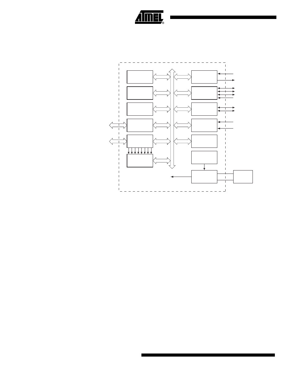
Block Diagram
Figure 4-1.
AT89LP216 Block Diagram
5.
Comparison to Standard 8051
The AT89LP216 is part of a family of devices with enhanced features that are fully binary com-
patible with the MCS-51 instruction set. In addition, most SFR addresses, bit assignments, and
pin alternate functions are identical to Atmel's existing standard 8051 products. However, due to
the high performance nature of the device, some system behaviors are different from those of
Atmel's standard 8051 products such as AT89S52 or AT89S2051. The differences from the
standard 8051 are outlined in the following paragraphs.
5.1
System Clock
The CPU clock frequency equals the external XTAL1 frequency. The oscillator is no longer
divided by 2 to provide the internal clock, and x2 mode is not supported.
5.2
Instruction Execution with Single-cycle Fetch
The CPU fetches one code byte from memory every clock cycle instead of every six clock
cycles. This greatly increases the throughput of the CPU. As a consequence, the CPU no longer
executes instructions in 12 to 48 clock cycles. Each instruction executes in only 1 to 4 clock
cycles.
See “Instruction Set Summary” on page 59.
for more details.
Single Cycle
8051 CPU
2K Bytes
Flash
128 Bytes
RAM
Port 3
Configurable I/O
Port 1
Configurable I/O
UART
SPI
Timer 0
Timer 1
Analog
Comparator
Watchdog
Timer
On-Chip
RC Oscillator
General-purpose
Interrupt
Configurable
Oscillator
CPU Clock
Crystal or
Resonator