Rainbow Electronics AT89LP216 User Manual
Page 50

50
3621A–MICRO–6/06
AT89LP216 [Preliminary]
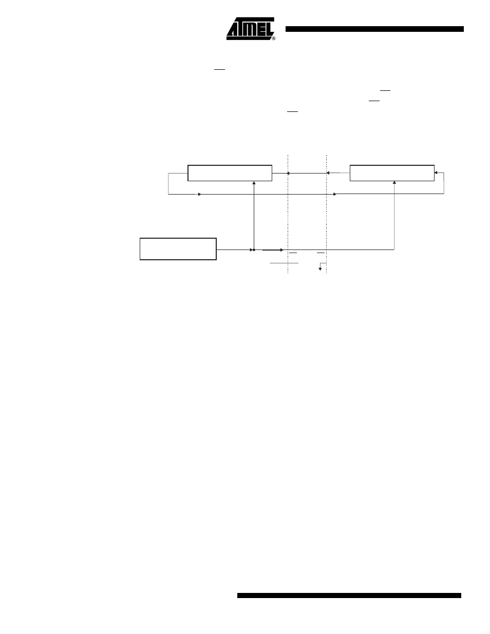
The interconnection between master and slave CPUs with SPI is shown in
. The four
pins in the interface are Master-In/Slave-Out (MISO), Master-Out/Slave-In (MOSI), Shift Clock
(SCK), and Slave Select (SS). The SCK pin is the clock output in master mode, but is the clock
input in slave mode. The MSTR bit in SPCR determines the directions of MISO and MOSI. Also
notice that MOSI connects to MOSI and MISO to MISO. In master mode, SS/P1.4 is ignored and
may be used as a general-purpose input or output. In slave mode, SS must be driven low to
select an individual device as a slave. When SS is driven high, the slave’s SPI port is deacti-
vated and the MOSI/P1.5 pin can be used as a general-purpose input.
Figure 18-1. SPI Master-slave Interconnection
The SPI has two modes of operation: normal (non-buffered write) and enhanced (buffered
write). In normal mode, writing to the SPI data register (SPDR) of the master CPU starts the SPI
clock generator and the data written shifts out of the MOSI pin and into the MOSI pin of the slave
CPU. Transmission may start after an initial delay while the clock generator waits for the next full
bit slot of the specified baud rate. After shifting one byte, the SPI clock generator stops, setting
the end of transmission flag (SPIF) and transferring the received byte to the read buffer (SPDR).
If both the SPI interrupt enable bit (SPIE) and the serial port interrupt enable bit (ES) are set, an
interrupt is requested. Note that SPDR refers to either the write data buffer or the read data
buffer, depending on whether the access is a write or read. In normal mode, because the write
buffer is transparent (and a write access to SPDR will be directed to the shift buffer), any attempt
to write to SPDR while a transmission is in progress will result in a write collision with WCOL set.
However, the transmission will still complete normally, but the new byte will be ignored and a
new write access to SPDR will be necessary.
Enhanced mode is similar to normal mode except that the write buffer holds the next byte to be
transmitted. Writing to SPDR loads the write buffer and sets WCOL to signify that the buffer is
full and any further writes will overwrite the buffer. WCOL is cleared by hardware when the buff-
ered byte is loaded into the shift register and transmission begins. If the master SPI is currently
idle, i.e. if this is the first byte, then after loading SPDR, transmission of the byte starts and
WCOL is cleared immediately. While this byte is transmitting, the next byte may be written to
SPDR. The Load Enable flag (LDEN) in SPSR can be used to determine when transmission has
started. LDEN is asserted during the first four bit slots of a SPI transfer. The master CPU should
first check that LDEN is set and that WCOL is cleared before loading the next byte. In enhanced
mode, if WCOL is set when a transfer completes, i.e. the next byte is available, then the SPI
immediately loads the buffered byte into the shift register, resets WCOL, and continues
transmission without stopping and restarting the clock generator. As long as the CPU can keep
the write buffer full in this manner, multiple bytes may be transferred with minimal latency
between bytes.
8-Bit Shift Register
8-Bit Shift Register
Master
Clock Generator
SPI
MISO
Slave
MISO
MOSI MOSI
SCK
SCK
SS
SS
V
CC
MSB
LSB
MSB
LSB
