Rainbow Electronics AT89LP216 User Manual
Page 51

51
3621A–MICRO–6/06
AT89LP216 [Preliminary]
Notes:
1. Set up the clock mode before enabling the SPI: set all bits needed in SPCR except the SPE bit, then set SPE.
2. Enable the master SPI prior to the slave device.
3. Slave echoes master on the next Tx if not loaded with new data.
Table 18-1.
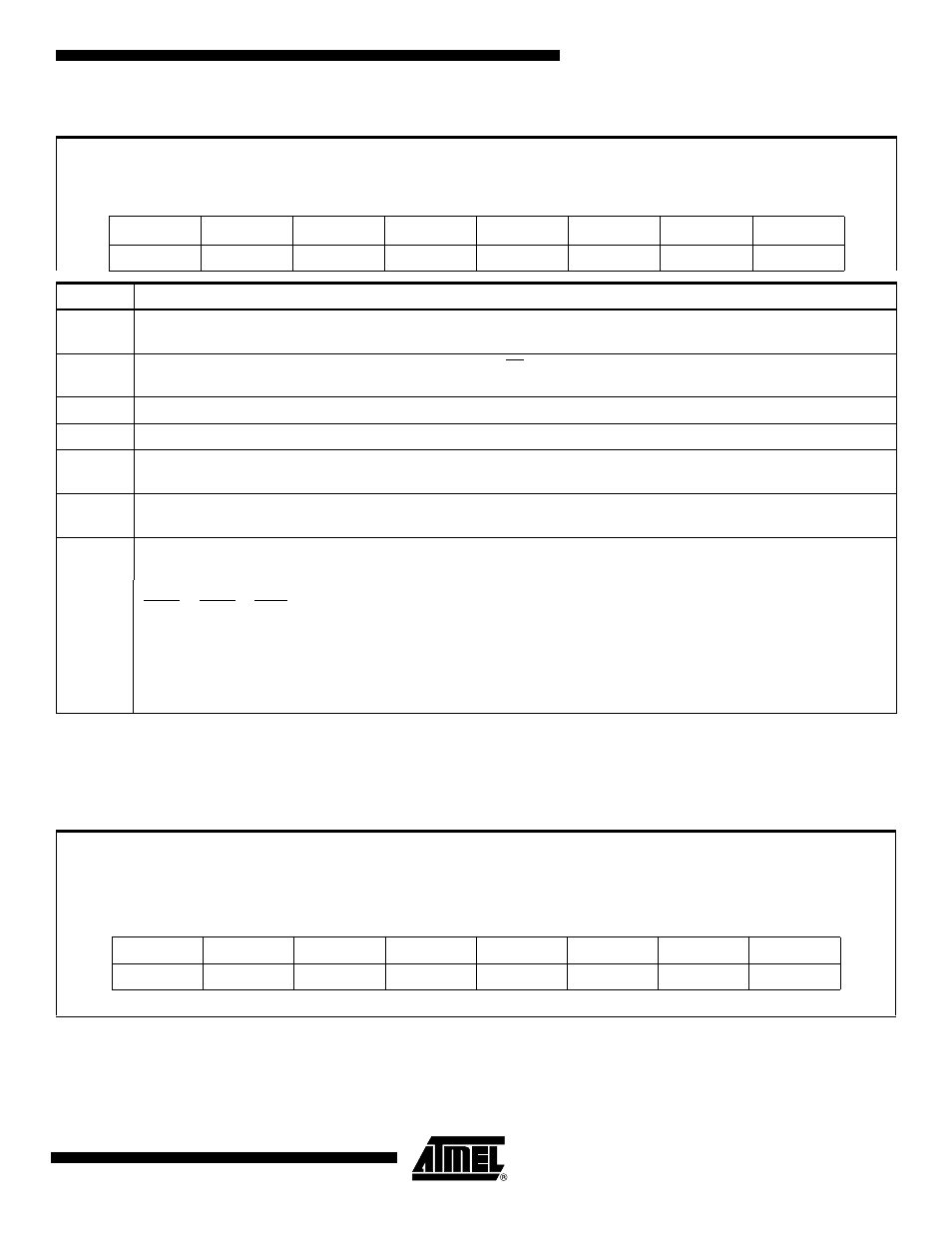
SPCR – SPI Control Register
SPCR Address = E9H
Reset Value = 0000 0000B
Not Bit Addressable
SPIE
SPE
DORD
MSTR
CPOL
CPHA
SPR1
SPR0
Bit
7
6
5
4
3
2
1
0
Symbol
Function
SPIE
SPI interrupt enable. This bit, in conjunction with the ES bit in the IE register, enables SPI interrupts: SPIE = 1 and ES = 1
enable SPI interrupts. SPIE = 0 disables SPI interrupts.
SPE
SPI enable. SPI = 1 enables the SPI channel and connects SS, MOSI, MISO and SCK to pins P1.4, P1.5, P1.6, and P1.7.
SPI = 0 disables the SPI channel.
DORD
Data order. DORD = 1 selects LSB first data transmission. DORD = 0 selects MSB first data transmission.
MSTR
Master/slave select. MSTR = 1 selects Master SPI mode. MSTR = 0 selects slave SPI mode.
CPOL
Clock polarity. When CPOL = 1, SCK is high when idle. When CPOL = 0, SCK of the master device is low when not
transmitting. Please refer to figure on SPI clock phase and polarity control.
CPHA
Clock phase. The CPHA bit together with the CPOL bit controls the clock and data relationship between master and
slave. Please refer to figure on SPI clock phase and polarity control.
SPR0
SPR1
SPI clock rate select. These two bits control the SCK rate of the device configured as master. SPR1 and SPR0 have no
effect on the slave. The relationship between SCK and the oscillator frequency, F
OSC.
, is as follows:
SPR1
SPR0
SCK
0
0
f
OSC
/4
0
1
f
OSC
/8
1
0
f
OSC
/32
1
1
f
OSC
/64
Table 18-2.
SPDR – SPI Data Register
SPDR Address = EAH
Reset Value = 00H (after cold reset)
unchanged (after warm reset)
Not Bit Addressable
SPD7
SPD6
SPD5
SPD4
SPD3
SPD2
SPD1
SPD0
Bit
7
6
5
4
3
2
1
0
