Memory programming, Program memory lock bits, Fuse bits – Rainbow Electronics ATtiny28L User Manual
Page 44: Signature bytes, Calibration byte, Programming the flash, Attiny28l/v
44
ATtiny28L/V
1062E–10/01
Memory
Programming
Program Memory Lock
Bits
The ATtiny28 MCU provides two Lock bits that can be left unprogrammed (“1”) or can be
programmed (“0”) to obtain the additional features listed in Table 20. The Lock bits can
only be erased with the Chip Erase command.
Note:
1. Further programming of the Fuse bits is also disabled. Program the Fuse bits before
programming the Lock bits.
Fuse Bits
The ATtiny28 has five Fuse bits, INTCAP and CKSEL3..0.
•
When the INTCAP Fuse is programmed (“0”), internal load capacitors are
connected between XTAL1/XTAL2 and GND, similar to C1 and C2 in Figure 2. See
“Crystal Oscillator” on page 4. Default value is unprogrammed (“1”).
•
CKSEL3..0 Fuses: See Table 1, “Device Clocking Option Select,” on page 4 and
Table 5, “ATtiny28 Clock Options and Start-up Time,” on page 14, for which
combination of CKSEL3..0 to use. Default value is “0010”, internal RC oscillator with
long start-up time.
The status of the Fuse bits is not affected by Chip Erase.
Signature Bytes
All Atmel microcontrollers have a 3-byte signature code that identifies the device. The
three bytes reside in a separate address space.
For the ATtiny28, they are:
1.
$000: $1E (indicates manufactured by Atmel)
2.
$001: $91 (indicates 2 KB Flash memory)
3.
$002: $07 (indicates ATtiny28 device when signature byte $001 is $91)
Calibration Byte
The ATtiny28 has one byte calibration value for the internal RC oscillator. This byte
resides in the high byte of address $000 in the signature address space. During memory
programming, the external programmer must read this location, and program it into a
selected location in the the normal Flash program memory. At start-up, the user soft-
ware must read this Flash location and write the value to the OSCCAL register.
Programming the Flash
Atmel’s ATtiny28 offers 2K bytes of Flash program memory.
The ATtiny28 is shipped with the on-chip Flash program memory array in the erased
state (i.e., contents = $FF) and ready to be programmed. This device supports a high-
voltage (12V) parallel programming mode. Only minor currents (<1mA) are drawn from
the +12V pin during programming.
The program memory array in the ATtiny28 is programmed byte-by-byte. During pro-
gramming, the supply voltage must be in accordance with Table 21.
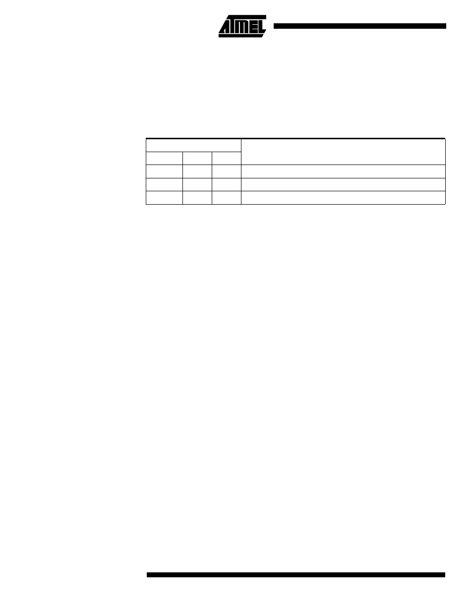
Table 20. Lock Bit Protection Modes
Memory Lock Bits
Protection Type
Mode
LB1
LB2
1
1
1
No memory lock features enabled.
2
0
1
Further programming of the Flash is disabled.
3
0
0
Same as mode 2, and verify is also disabled.