I/o ports, Port a, Port a data register – porta – Rainbow Electronics ATtiny28L User Manual
Page 36: Port a control register – pacr, Attiny28l/v, 8v (v

36
ATtiny28L/V
1062E–10/01
I/O Ports
All AVR ports have true read-modify-write functionality when used as general digital I/O
ports. This means that the direction of one port pin can be changed without unintention-
ally changing the direction of any other pin with the SBI and CBI instructions. The same
applies for changing drive value (if configured as output) or enabling/disabling of pull-up
resistors (if configured as input).
Port A
Port A is a 4-bit I/O port. PA2 is output-only, while PA3, PA1 and PA0 are bi-directional.
Three I/O memory address locations are allocated for Port A, one each for the Data
Register – PORTA, $1B, Port A Control Register – PACR, $1A and the Port A Input Pins
– PINA, $19. The Port A Input Pins address is read-only, while the Data Register and
the Control Register are read/write. Compared to other output ports, the Port A output is
delayed one extra clock cycle.
Port pins PA0, PA1 and PA3 have individually selectable pull-up resistors. When pins
PA0, PA1 or PA3 are used as inputs and are externally pulled low, they will source cur-
rent if the internal pull-up resistors are activated. PA2 is output-only. The PA2 output
buffer can sink 25 mA and thus drive a high-current LED directly. This output can also
be modulated (see “Hardware Modulator” on page 29 for details).
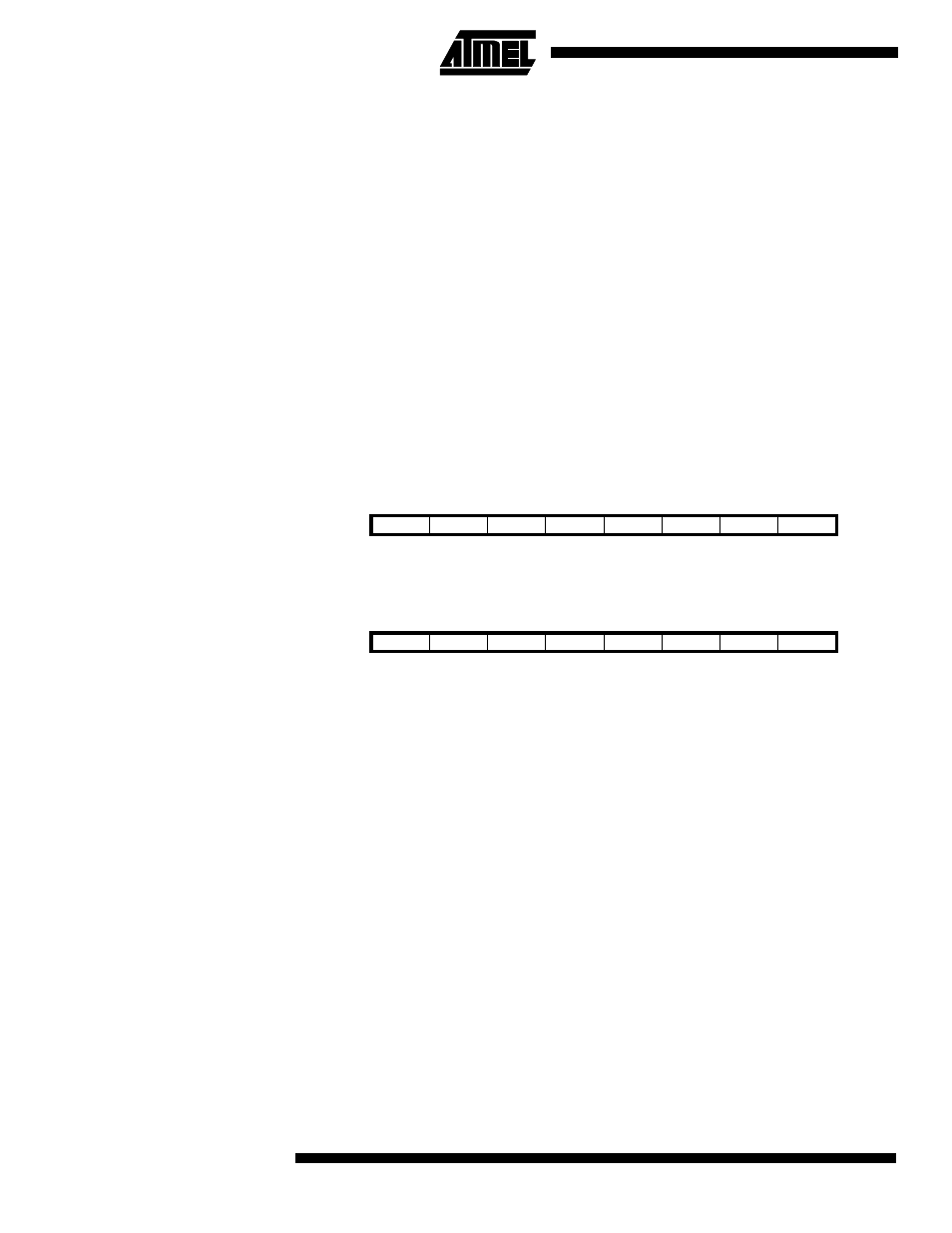
Port A Data Register – PORTA
Port A Control Register –
PACR
• Bits 7..4 – Res: Reserved Bits
These bits are reserved bits in the ATtiny28 and always read as zero.
• Bit 3 – DDA3: Data Direction PA3
When DDA3 is set (one), the corresponding pin is an output pin. Otherwise, it is an input
pin.
• Bit 2 – PA2HC: PORTA2 High Current Enable
When the PA2HC bit is set (one), an additional driver at the output pin PA2 is enabled.
This makes it possible to sink 25 mA at V
CC
= 1.8V (V
OL
= 0.8V). When the PA2HC bit is
cleared (zero), PA2 can sink 15 mA at V
CC
= 1.8V (V
OL
= 0.8V).
• Bits 1, 0 – DDA1, DDA0: Data Direction PA1 and PA0
When DDAn is set (one), the corresponding pin is an output pin. Otherwise, it is an input
pin.
Bit
7
6
5
4
3
2
1
0
$1B
–
–
–
–
PORTA3
PORTA2
PORTA1
PORTA0
PORTA
Read/Write
R
R
R
R
R/W
R/W
R/W
R/W
Initial Value
0
0
0
0
0
1
0
0
Bit
7
6
5
4
3
2
1
0
$1A
–
–
–
–
DDA3
PA2HC
DDA1
DDA0
PACR
Read/Write
R
R
R
R
R/W
R/W
R/W
R/W
Initial Value
0
0
0
0
0
0
0
0
