Port d, Port d data register – portd, Port d data direction register – ddrd – Rainbow Electronics ATtiny28L User Manual
Page 42: Port d input pins address – pind, Attiny28l/v

42
ATtiny28L/V
1062E–10/01
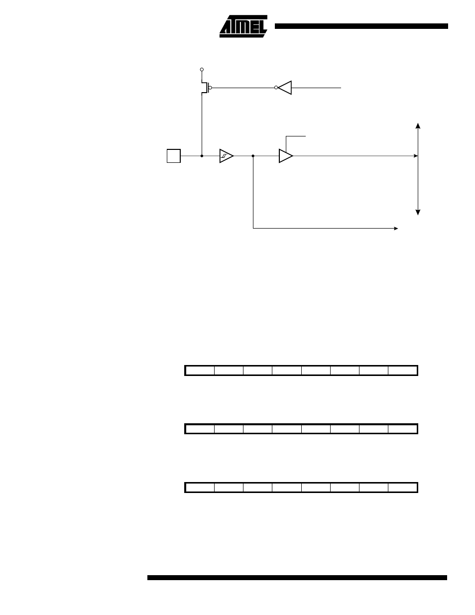
Figure 34. PORT B Schematic Diagram (Pins PB7 - PB5)
Port D
Port D is an 8-bit bi-directional I/O port with internal pull-up resistors.
Three I/O memory address locations are allocated for Port D, one each for the Data
Register – PORTD, $12, Data Direction Register – DDRD, $11 and the Port D Input Pins
– PIND, $10. The Port D Input Pins address is read-only, while the Data Register and
the Data Direction Register are read/write.
The Port D output buffers can sink 10 mA. As inputs, Port D pins that are externally
pulled low will source current if the pull-up resistors are activated.
Port D Data Register – PORTD
Port D Data Direction Register
– DDRD
Port D Input Pins Address –
PIND
The Port D Input Pins Address (PIND) is not a register; this address enables access to
the physical value on each Port D pin. When reading PORTD, the Port D Data Latch is
read and when reading PIND, the logical values present on the pins are read.
DA
T
A
BUS
PBn
TO LOW-LEVEL DETECTOR
RP:
n:
READ PORT B PIN
5 - 7
RP
MOS
PULL-
UP
PULL-UP PORT B
Bit
7
6
5
4
3
2
1
0
$12
PORTD7
PORTD6
PORTD5
PORTD4
PORTD3
PORTD2
PORTD1
PORTD0
PORTD
Read/Write
R/W
R/W
R/W
R/W
R/W
R/W
R/W
R/W
Initial Value
0
0
0
0
0
0
0
0
Bit
7
6
5
4
3
2
1
0
$11
DDD7
DDD6
DDD5
DDD4
DDD3
DDD2
DDD1
DDD0
DDRD
Read/Write
R/W
R/W
R/W
R/W
R/W
R/W
R/W
R/W
Initial Value
0
0
0
0
0
0
0
0
Bit
7
6
5
4
3
2
1
0
$10
PIND7
PIND6
PIND5
PIND4
PIND3
PIND2
PIND1
PIND0
PIND
Read/Write
R
R
R
R
R
R
R
R
Initial Value
N/A
N/A
N/A
N/A
N/A
N/A
N/A
N/A
