Port b schematics, Attiny28l/v – Rainbow Electronics ATtiny28L User Manual
Page 40
40
ATtiny28L/V
1062E–10/01
• T0 – Port B, Bit 2
T0, Timer/Counter0 Counter source. See the timer description for further details. If T0 is
used as the counter source, the pull-up resistor on PB2 is disabled and PB2 will not give
low-level interrupts.
• AIN1 – Port B, Bit 1
AIN1, Analog Comparator Negative input. When the on-chip analog comparator is
enabled, this pin also serves as the negative input of the comparator. If the analog com-
parator is enabled, the pull-up resistors on PB1 and PB0 are disabled and these pins will
not give low-level interrupts.
• AIN0 – Port B, Bit 0
AIN0, Analog Comparator Positive input. When the on-chip analog comparator is
enabled, this pin also serves as the positive input of the comparator. If the analog com-
parator is enabled, the pull-up resistors on PB1 and PB0 are disabled and these pins will
not give low-level interrupts.
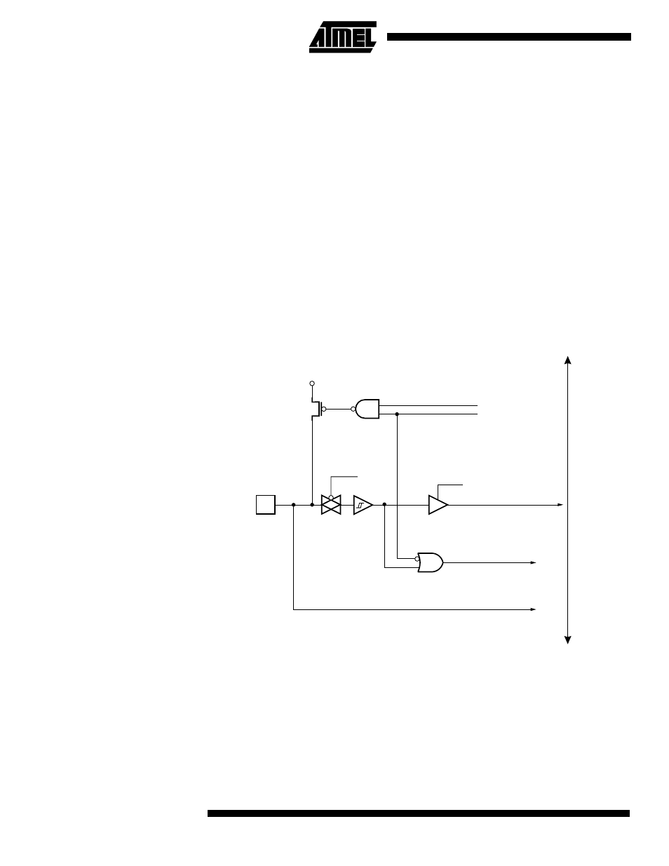
Port B Schematics
Note that all port pins are synchronized. The synchronization latches are, however, not
shown in the figures.
Figure 31. Port B Schematic Diagram (Pins PB0 and PB1)
DA
T
A
BUS
MOS
PULL-
UP
PBn
RP: READ PORTB PIN
n : 0, 1
PULL-UP PORT B
COMPARATOR DISABLE
RP
TO LOW-LEVEL DETECTOR
TO COMPARATOR
AINn
PWRDN