Hardware modulator, Modulation control register – modcr, Attiny28l/v – Rainbow Electronics ATtiny28L User Manual
Page 29

29
ATtiny28L/V
1062E–10/01
Hardware Modulator
ATtiny28 features a built-in hardware modulator connected to a high-current output pad,
PA2. The hardware modulator generates a configurable pulse train. The on-time of a
pulse can be set to a number of chip clock cycles. This is done by configuring the Modu-
lation Control Register (MODCR).
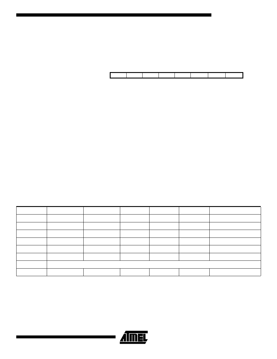
Modulation Control Register –
MODCR
• Bits 7..3 – ONTIM4..0: Modulation On-time
This 5-bit value +1 determines the number of clock cycles the output pin PA2 is active
(low).
• Bits 2..0 – MCONF2..0: Modulation Configuration Bits 2, 1 and 0
These three bits determine the relationship between the on- and off-times of the modu-
lator, and thereby the duty-cycle. The various settings are shown in Table 13. The
minimum and maximum modulation period is also shown in the table. The minimum
modulation period is obtained by setting ONTIM to zero, while the maximum period is
obtained by setting ONTIM to 31. The configuration values for some common oscillator
and carrier frequencies are listed in Table 15. The relationship between oscillator fre-
quency and carrier frequency is:
If the MCONF register is set to 111, the carrier frequency will be equal to the oscillator
frequency.
Note:
In the high-frequency mode, the output is gated with the clock signal. Thus, the on- and off-times will be dependent on the clock
input to the MCU. Also note that when changing from this mode directly to another modulation mode, the output will have a
small glitch. Thus, PA2 should be set to stop the modulated output before changing from this mode.
Bit
7
6
5
4
3
2
1
0
$02
ONTIM4
ONTIM3
ONTIM2
ONTIM1
ONTIM0
MCONF2
MCONF1
MCONF0
MODCR
Read/Write
R/W
R/W
R/W
R/W
R/W
R/W
R/W
R/W
Initial Value
0
0
0
0
0
0
0
0
fcarrier
fosc
On-time
Off-time
+
(
)
-----------------------------------------------------
=
Table 13. MCONF2..0 Effect on Duty-cycle and Modulation Period
MCONF2..0
On-time
Off-time
Duty-cycle
Min Period
Max Period
Comment
000
X
X
100%
X
X
Unmodulated output
001
ONTIM+1
ONTIM+1
50%
2 CK
64 CK
010
ONTIM+1
2 x (ONTIM+1)
33%
3 CK
96 CK
011
ONTIM+1
3 x (ONTIM+1)
25%
4 CK
128 CK
100
2 x (ONTIM+1)
ONTIM+1
67%
3 CK
96 CK
101
3 x (ONTIM+1)
ONTIM+1
75%
4 CK
128 CK
110
Reserved
111
X
X
Note 1
1 CK
1 CK
High-frequency output
