Port a as general digital i/o, Port a input pins address – pina, Alternate function of pa2 – Rainbow Electronics ATtiny28L User Manual
Page 37: Attiny28l/v
37
ATtiny28L/V
1062E–10/01
Port A as General Digital I/O
PA3, PA1 and PA0 are general I/O pins. The DDAn (n: 3,1,0) bits in PACR select the
direction of these pins. If DDAn is set (one), PAn is configured as an output pin. If DDAn
is cleared (zero), PAn is configured as an input pin. If PORTAn is set (one) when the pin
is configured as an input pin, the MOS pull-up resistor is activated. To switch the pull-up
resistor off, the PORTAn bit has to be cleared (zero) or the pin has to be configured as
an output pin. The effects of the DDAn and PORTAn bits on PA3, PA1 and PA0 are
shown in Table 17. The port pins are tri-stated when a reset condition becomes active,
even if the clock is not running.
Note:
n: 3,1,0, pin number
Port A Input Pins Address –
PINA
The Port A Input Pins address (PINA) is not a register; this address enables access to
the physical value on each Port A pin. When reading PORTA, the Port A Data Latch is
read and when reading PINA, the logical values present on the pins are read.
Alternate Function of PA2
PA2 is the built-in, high-current LED driver and it is always an output pin. The output sig-
nal can be modulated with a software programmable frequency. See “Hardware
Modulator” on page 29 for further details.
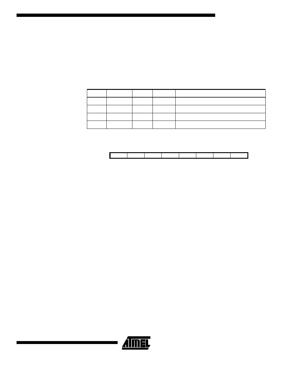
Table 17. DDAn Effects on Port A Pins
DDAn
PORTAn
I/O
Pull-up
Comment
0
0
Input
No
Tri-state (high-Z)
0
1
Input
Yes
PAn will source current if ext. pulled low.
1
0
Output
No
Push-pull Zero Output
1
1
Output
No
Push-pull One Output
Bit
7
6
5
4
3
2
1
0
$19
–
–
–
–
PINA3
–
PINA1
PINA0
PINA
Read/Write
R
R
R
R
R
R
R
R
Initial Value
0
0
0
0
N/A
0
N/A
N/A