Polling circuit and control logic, Basic clock cycle of the digital circuitry – Rainbow Electronics T5761 User Manual
Page 8
8
T5760/T5761
4561B–RKE–10/02
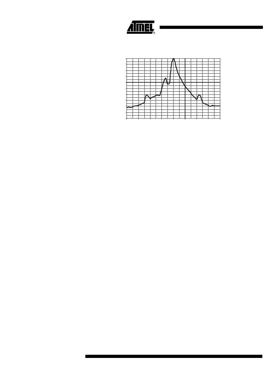
Figure 7.
Wide Band Receiving Frequency Response
Polling Circuit and
Control Logic
The receiver is designed to consume less than 1 mA while being sensitive to signals
from a corresponding transmitter. This is achieved via the polling circuit. This circuit
enables the signal path periodically for a short time. During this time the bit-check logic
verifies the presence of a valid transmitter signal. Only if a valid signal is detected, the
receiver remains active and transfers the data to the connected microcontroller. If there
is no valid signal present, the receiver is in sleep mode most of the time resulting in low
current consumption. This condition is called polling mode. A connected microcontroller
is disabled during that time.
All relevant parameters of the polling logic can be configured by the connected micro-
controller. This flexibility enables the user to meet the specifications in terms of current
consumption, system response time, data rate etc.
Regarding the number of connection wires to the microcontroller, the receiver is very
flexible. It can be either operated by a single bi-directional line to save ports to the
connected microcontroller or it can be operated by up to five uni-directional ports.
Basic Clock Cycle of
the Digital Circuitry
The complete timing of the digital circuitry and the analog filtering is derived from one
clock. This clock cycle T
Clk
is derived from the crystal oscillator (XTO) in combination
with a divide by 14 circuit. According to chapter ‘RF Front End’, the frequency of the
crystal oscillator (f
XTO
) is defined by the RF input signal (f
RFin
) which also defines the
operating frequency of the local oscillator (f
LO
). The basic clock cycle is T
Clk
= 14/f
XTO
giving T
Clk
= 2.066 µs for f
RF
= 868.3 MHz and T
Clk
= 1.961 µs for f
RF
= 915 MHz.
T
Clk
controls the following application-relevant parameters:
•
Timing of the polling circuit including bit check
•
Timing of the analog and digital signal processing
•
Timing of the register programming
•
Frequency of the reset marker
•
IF filter center frequency (f
IF0
)
Most applications are dominated by two transmission frequencies: f
Transmit
= 915 MHz is
mainly used in USA, f
Transmit
= 868.3 MHz in Europe. In order to ease the usage of all
T
Clk
-dependent parameters on this electrical characteristics display three conditions for
each parameter.
-100.0
-90.0
-80.0
-70.0
-60.0
-50.0
-40.0
-30.0
-20.0
-10.0
0.0
-12.0
-9.0
-6.0
-3.0
0.0
3.0
6.0
9.0
12.0
df (MHz)
dP (dB)