Programming the configuration register – Rainbow Electronics T5761 User Manual
Page 25
25
T5760/T5761
4561B–RKE–10/02
Programming the Configuration Register
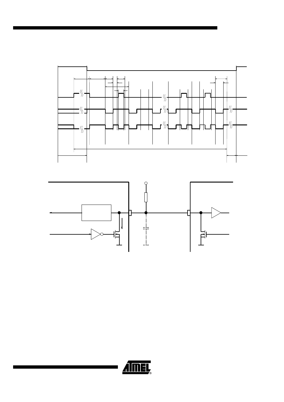
Figure 31.
Timing of the Register Programming
Figure 32.
Data Interface
The configuration registers are programmed serially via the bi-directional data line
according to Figure 31 and Figure 32.
To start programming, the serial data line DATA is pulled to Low for the time period t1 by
the microcontroller. When DATA has been released, the receiver becomes the master
device. When the programming delay period t2 has elapsed, it emits 15 subsequent
synchronization pulses with the pulse length t3. After each of these pulses, a program-
ming window occurs. The delay until the program window starts is determined by t4, the
duration is defined by t5. Within the programming window, the individual bits are set. If
the microcontroller pulls down Pin DATA for the time period t7 during t5, the according
bit is set to ’0’. If no programming pulse t7 is issued, this bit is set to ’1’. All 15 bits are
subsequently programmed this way. The time frame to program a bit is defined by t6.
Out1
(microcontroller)
Data_out (DATA)
Serial bi-directional
data line
X
Bit 1
("0")
Bit 2
("1")
Bit 14
("0")
Bit 15
("0")
X
t1
t2
t3
t4
t5
t6
t8
t7
Programming frame
(Start bit)
(Register-
select)
(Poll8)
(Stop bit)
Receiving
mode
Start-up
mode
t9
IC_ACTIVE
TSleep TStart-up
Sleep
mode
Data_In
Data_out
Input -
Interface
DATA
0 ... 20 V
0 V / 5 V
V
X
= 5 V to 20 V
R
pup
C
L
V S = 4.5 V to 5.5 V
I/O
Serial bi-directional data line
T5760/
T5761
Microcontroller
Out1 (microcontroller )
I
D