Figure 15 and figure 16, Figure 15 t, Figure 16 – Rainbow Electronics T5761 User Manual
Page 14: Figure 16 gi, Switching the receiver back to sleep mode
14
T5760/T5761
4561B–RKE–10/02
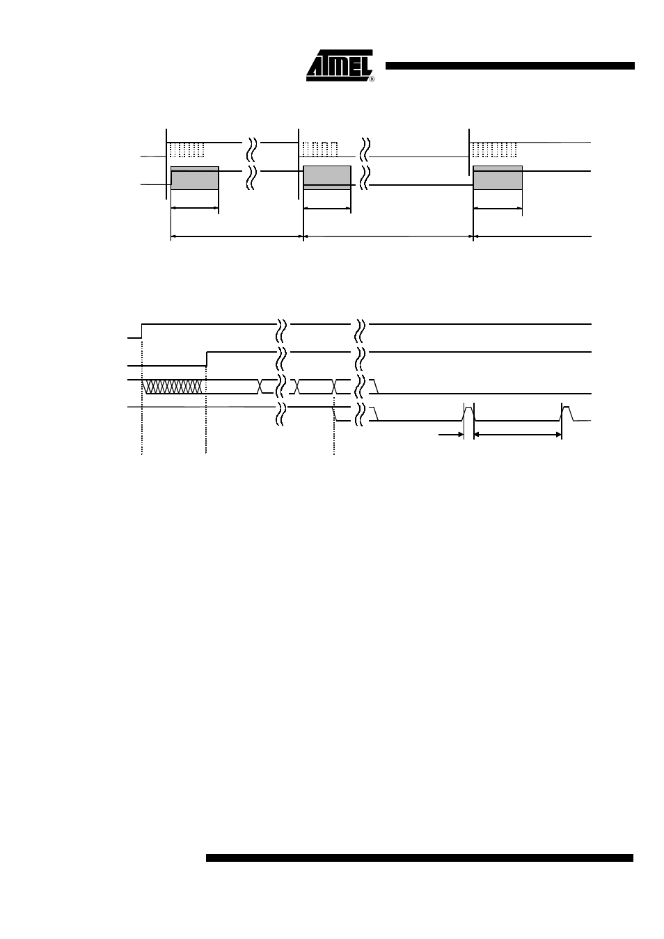
Figure 15.
Debouncing of the Demodulator Output
Figure 16.
Steady L State Limited DATA Output Pattern After Transmission
After the end of a data transmission, the receiver remains active. Depending of the bit
Noise_Disable in the OPMODE register, the output signal at Pin DATA is high or
random noise pulses appear at Pin DATA (see chapter ’Digital Noise Suppression’). The
edge-to-edge time period t
ee
of the majority of these noise pulses is equal or slightly
higher than T
DATA_min
.
Switching the Receiver
Back to Sleep Mode
The receiver can be set back to polling mode via Pin DATA or via Pin POLLING/_ON.
When using Pin DATA, this pin must be pulled to Low for the period t1 by the connected
microcontroller. Figure 17 illustrates the timing of the OFF command (see Figure 32).
The minimum value of t1 depends on BR_Range. The maximum value for t1 is not
limited but it is recommended not to exceed the specified value to prevent erasing the
reset marker. Note also that an internal reset for the OPMODE and the LIMIT register
will be generated if t1 exceeds the specified values. This item is explained in more detail
in the chapter ‘Configuration of the Receiver’. Setting the receiver to sleep mode via
DATA is achieved by programming bit 1 to be ‘1’ during the register configuration. Only
one sync pulse (t3) is issued.
The duration of the OFF command is determined by the sum of t1, t2 and t10. After the
OFF command the sleep time T
Sleep
elapses. Note that the capacitive load at Pin DATA
is limited (see chapter ’Data Interface’).
Data_out (DATA)
Dem_out
t
ee
t
ee
t
DATA_min
t
ee
t
DATA_min
t
DATA_min
Bit check
IC_ACTIVE
Data_out (DATA)
Start-up mode
Receiving mode
t
DATA_L_max
t
DATA_min
Bit-check mode
Dem_out