Rf front end – Rainbow Electronics T5761 User Manual
Page 4
4
T5760/T5761
4561B–RKE–10/02
RF Front End
The RF front end of the receiver is a low-IF heterodyne configuration that converts the
input signal into a 950 kHz/1 MHz IF signal with an image rejection of typical 30 dB.
According to Figure 3 the front end consists of an LNA (Low Noise Amplifier), LO (Local
Oscillator), I/Q mixer, polyphase lowpass filter and an IF amplifier.
The PLL generates the carrier frequency for the mixer via a full integrated synthesizer
with integrated low noise LC-VCO (Voltage Controlled Oscillator) and PLL-loop filter.
The XTO (crystal oscillator) generates the reference frequency f
XTO
. The integrated LC-
VCO generates two times the mixer drive frequency f
VCO
. The I/Q signals for the mixer
are generated with a divide by two circuit (f
LO
= f
VCO
/2). f
VCO
is divided by a factor of 256
and feeds into a phase frequency detector and compared with f
XTO
. The output of the
phase frequency detector is fed into an integrated loop filter and thereby generates the
control voltage for the VCO. If f
LO
is determined, f
XTO
can be calculated using the follow-
ing formula:
f
XTO
= f
LO
/128
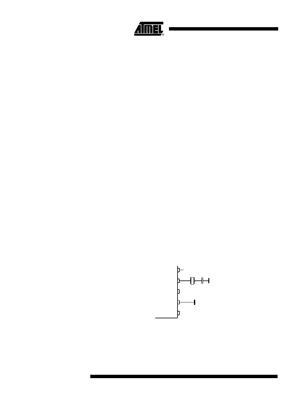
The XTO is a one-pin oscillator that operates at the series resonance of the quartz
crystal with high current but low voltage signal, so that there is only a small voltage at
the crystal oscillator frequency at Pin XTAL. According to Figure 4, the crystal should be
connected to GND with a series capacitor C
L
. The value of that capacitor is recom-
mended by the crystal supplier. Due to a somewhat inductive impedance at steady state
oscillation and some PCB parasitics a lower value of C
L
is normally necessary.
The value of C
L
should be optimized for the individual board layout to achieve the exact
value of f
XTO
(the best way is to use a crystal with known load resonance frequency to
find the right value for this capacitor) and hereby of f
LO
. When designing the system in
terms of receiving bandwidth and local oscillator accuracy, the accuracy of the crystal
and the XTO must be considered.
If a crystal with ±30 ppm adjustment tolerance at 25
°
C, ±50 ppm over temperature
-40
°
C to +105
°
C, ±10 ppm of total aging and a CM (motional capacitance) of 7 fF is
used, an additional XTO pulling of ±30 ppm has to be added.
The resulting total LO tolerance of ±120 ppm agrees with the receiving bandwidth
specification of the T5760/T5761 if the T5750 has also a total LO tolerance of
±120 ppm.
Figure 4.
XTO Peripherals
The nominal frequency f
LO
is determined by the RF input frequency f
RF
and the IF
frequency f
IF
using the following formula (low side injection):
f
LO
= f
RF
- f
IF
DVCC
XTAL
TEST 3
TEST 2
n.c.
V
S
C
L