Functional diagram detailed description, Control and status registers – Rainbow Electronics MAX9452 User Manual
Page 7

MAX9450/MAX9451/MAX9452
High-Precision Clock Generators
with Integrated VCXO
_______________________________________________________________________________________
7
GNDA
V
DDA
V
DD
GND
VCXO
CRYSTAL
5MHz TO 160MHz
FUNDAMENTAL MODE
AND AT CUT
LOCK DET
1/M
LUT FOR P
LOOP FILTER
RJ
LP2
LP1
X1
X2
I
2
C PORT
SCL
SDA
LUT FOR N1, N2
LUT FOR M
AD0
AD1
IN0+
IN0-
IN1+
IN1-
SEL0
0
1
CLK
MONITOR
CMON
INT
1/N1
CLK1+
CLK1-
OE
CLK0+
CLK0-
1/N0
1/P
PFD/CP
SEL1
MR
SPI PORT
CONTROL
REGISTERS
GND/CS
MUX
LOCK
12k
Ω TO 200kΩ
DIV0
DIV1
MAX9450
MAX9451
MAX9452
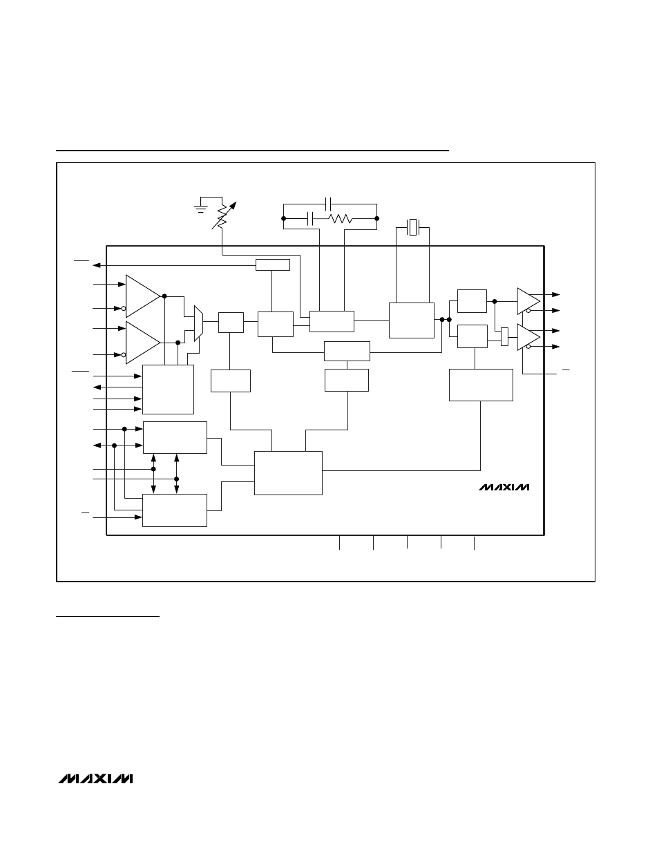
Functional Diagram
Detailed Description
The MAX9450/MAX9451/MAX9452 clock generators
provide high-precision clocks for timing in SONET/SDH
systems or Gigabit Ethernet systems. The MAX9450/
MAX9451/MAX9452 can also provide clocks for the
high-speed and high-resolution ADCs and DACs in 3G
base stations. Additionally, the MAX9450/MAX9451/
MAX9452 can be used as a jitter attenuator for generat-
ing high-precision clock signals.
The MAX9450/MAX9451/MAX9452 feature two differen-
tial inputs and two differential clock outputs. The inputs
accept LVPECL, LVDS, and LVCMOS signals. The
input reference clock ranges from 8kHz to 500MHz and
the output clock ranges from 15MHz to 160MHz. The
internal clock monitor observes the condition of the
input reference clocks and provides a hitless switch
when an input failure is detected. The MAX9450/
MAX9451/MAX9452 also provide holdover in case no
input clock is supplied.
Control and Status Registers
The MAX9450/MAX9451/MAX9452 contain eight 8-bit
control registers named CR0 to CR7. The registers are
accessible through the I
2
C/SPI interface. CR0 is for the
frequency-dividing factor, P. CR1 and CR2 hold the
values of the divider, M. CR3 and CR4 are for dividers
