Rainbow Electronics MAX9452 User Manual
Page 11

MAX9450/MAX9451/MAX9452
High-Precision Clock Generators
with Integrated VCXO
______________________________________________________________________________________
11
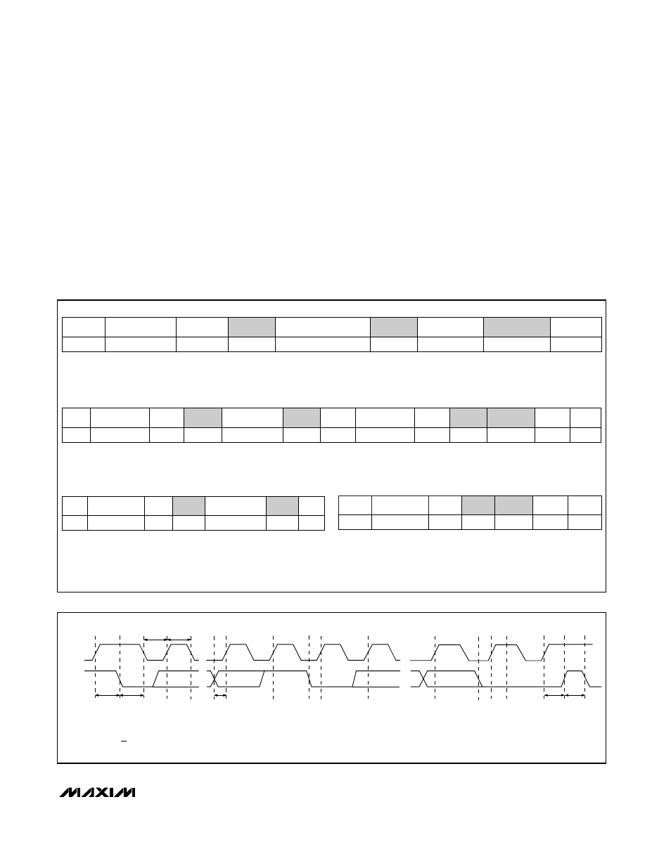
Data Transfer and Acknowledge
Following the START condition, each SCL clock pulse
transfers one bit. Between a START and a STOP, multiple
bytes can be transferred on the 2-wire bus. The first
seven bits (B0–B6) are for the device address. The eighth
bit (B7) indicates the writing (low) or reading (high) oper-
ation (W/R). The ninth bit (B8) is the ACK for the address
and operation type. A low ACK bit indicates a successful
transfer; otherwise, a high ACK bit indicates an unsuc-
cessful transfer. The next eight bits (register address),
B9–B16, form the address byte for the control register
to be written (Figure 4). The next bit, bit 17, is the ACK
for the register address byte. The following byte (Data1)
is the content to be written into the addressed register
of the slave. After this, the address counter of I
2
C is
increased by 1 (Rgst Addr + 1) and the next byte
(Data2) writes into a new register. To read the contents
in the MAX9450/MAX9451/MAX9452’s control registers,
the master sends the register address to be read to the
slave by a writing operation. Then it sends the byte of
device address + R to the slave. The slave (MAX9450/
MAX9451/MAX9452) responds with the content bytes
from the registers, starting from the pointed register to
the last register, CR8, consecutively back to the master
(Figure 5).
SMBCLK
A = START CONDITION
B = MSB OF ADDRESS CLOCKED INTO SLAVE
C = LSB OF ADDRESS CLOCKED INTO SLAVE
D = R/W BIT CLOCKED INTO SLAVE
A
B
C
D
E
F
G
H
I
J
SMBDATA
t
SU:STA
t
HD:STA
t
LOW
t
HIGH
t
SU:DAT
t
SU:STO
t
BUF
L
M
K
E = SLAVE PULLS SMBDATA LINE LOW
F = ACKNOWLEDGE BIT CLOCKED INTO MASTER
G = MSB OF DATA CLOCKED INTO SLAVE
H = LSB OF DATA CLOCKED INTO SLAVE
I = MASTER PULLS DATA LINE LOW
J = ACKNOWLEDGE CLOCKED INTO SLAVE
K = ACKNOWLEDGE CLOCK PULSE
L = STOP CONDITION
M = NEW START CONDITION
Figure 5. SMBus Write Timing Diagram
Write Byte Format
Read Byte Format
Send Byte Format
Receive Byte Format
Slave address: equiva-
lent to chip-select line of
a 3-wire interface
Command byte: selects to
which register you are writing
Slave address: equivalent
to chip-select line
Command byte: selects
from which register you
are reading
Slave address: repeated
due to change in data-
flow direction
Data byte: reads from
the register set by the
command byte
Command byte: sends com-
mand with no data, usually
used for one-shot command
Data byte: reads data from the register
commanded by the last read byte or
write byte transmission; also used for
SMBus alert response return address
S = Start condition Shaded = Slave transmission
P = Stop condition /// = Not acknowledged
Figure 4. I
2
C Interface Data Structure
S
ADDRESS
RD
ACK
DATA
///
P
—
7 bits
—
—
8 bits
—
—
WR
S
ACK
COMMAND
ACK
P
—
—
—
8 bits
—
—
ADDRESS
7 bits
P
1
ACK
—
DATA
8 bits
ACK
—
COMMAND
8 bits
ACK
—
S
ADDRESS
WR
ACK
COMMAND
ACK
S
ADDRESS
7 bits
—
—
8 bits
—
—
7 bits
—
RD
—
ACK
—
DATA
8 bits
///
—
P
—
Data byte: data goes into the register
set by the command byte (to set
thresholds, configuration masks, and
sampling rate)
WR
—
ADDRESS
7 bits
S
—
