Rainbow Electronics MAX9452 User Manual
General description, Applications, Features

General Description
The MAX9450/MAX9451/MAX9452 clock generators
provide high-precision clocks for timing in SONET/SDH
systems or Gigabit Ethernet systems. The MAX9450/
MAX9451/MAX9452 can also provide clocks for the high-
speed and high-resolution ADCs and DACs in 3G base
stations. Additionally, the devices can also be used as a
jitter attenuator for generating high-precision CLK signals.
The MAX9450/MAX9451/MAX9452 feature an integrated
VCXO. This configuration eliminates the use of an exter-
nal VCXO and provides a cost-effective solution for gen-
erating high-precision clocks. The MAX9450/MAX9451/
MAX9452 feature two differential inputs and clock out-
puts. The inputs accept LVPECL, LVDS, differential sig-
nals, and LVCMOS. The input reference clocks range
from 8kHz to 500MHz.
The MAX9450/MAX9451/MAX9452 offer LVPECL, HSTL,
and LVDS outputs, respectively. The output range is up
to 160MHz, depending on the selection of crystal. The
input and output frequency selection is implemented
through the I
2
C* or SPI™ interface. The MAX9450/
MAX9451/MAX9452 feature clock output jitter less than
0.8ps RMS (in a 12kHz to 20MHz band) and phase-
noise attenuation greater than -130dBc/Hz at 100kHz.
The phase-locked loop (PLL) filter can be set externally,
and the filter bandwidth can vary from 1Hz to 20kHz.
The MAX9450/MAX9451/MAX9452 feature an input
clock monitor with a hitless switch. When a failure is
detected at the selected reference clock, the device
can switch to the other reference clock. The reaction to
the recovery of the failed reference clock can be
revertive or nonrevertive. If both reference clocks fail,
the PLL retains its nominal frequency within a range of
±20ppm at +25°C.
The MAX9450/MAX9451/MAX9452 operate from
a 2.4V to
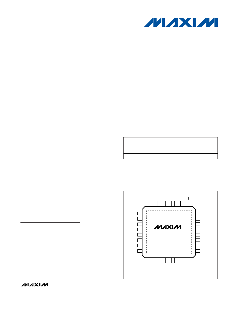
3.6V supply and are available in 32-pin TQFP packages
with exposed pads.
Applications
SONET/SDH Systems
10 Gigabit Network Routers and Switches
3G Cellular Phone Base Stations
General Jitter Attenuation
*Purchase of I
2
C components from Maxim Integrated Products,
Inc., or one of its sublicensed Associated Companies, conveys
a license under the Philips I
2
C Patent Rights to use these com-
ponents in an I
2
C system, provided that the system conforms to
the I
2
C Standard Specification as defined by Philips.
SPI is a trademark of Motorola, Inc.
Features
♦ Integrated VCXO Provides a Cost-Effective
Solution for High-Precision Clocks
♦ 8kHz to 500MHz Input Frequency Range
♦ 15MHz to 160MHz Output Frequency Range
♦ I
2
C or SPI Programming for the Input and Output
Frequency Selection
♦ PLL Lock Range > ±60ppm
♦ Two Differential Outputs with Three Types of
Signaling: LVPECL, LVDS, or HSTL
♦ Input Clock Monitor with Hitless Switch
♦ Internal Holdover Function within ±20ppm of the
Nominal Frequency
♦ Low Output CLK Jitter: < 0.8ps RMS in the 12kHz
to 20MHz Band
♦ Low Phase Noise > -130dBc at 100kHz
MAX9450/MAX9451/MAX9452
High-Precision Clock Generators
with Integrated VCXO
________________________________________________________________ Maxim Integrated Products
1
Ordering Information
19-0547; Rev 0; 5/06
For pricing, delivery, and ordering information, please contact Maxim/Dallas Direct! at
1-888-629-4642, or visit Maxim’s website at www.maxim-ic.com.
Note: All devices are specified over the -40°C to +85°C
temperature range.
+Denotes lead-free package.
**EP = Exposed pad.
†Future product—contact factory for availability.
PART
PIN-PACKAGE
OUTPUT
PKG CODE
MAX9450EHJ+
32 TQFP-EP**
LVPECL
H32E-6
MAX9451EHJ+†
32 TQFP-EP**
HSTL
H32E-6
MAX9452EHJ+†
32 TQFP-EP**
LVDS
H32E-6
MAX9450
MAX9451
MAX9452
TQFP
(5mm x 5mm)
TOP VIEW
EXPOSED PAD
(GND)
24
20
21
22
23
17
18
19
CLK1+
CLK1-
GND
CLK0+
V
DDQ
CLK0-
V
DDQ
OE
2
5
7
6
8
3
4
1
+
SEL0
IN0-
IN0+
IN1+
V
DD
9
10
11
12
13
14
15
AD1
16
AD0
SDA
SCL
MR
INT
26
27
28
29
30
31
32
RJ
GNDA
LP2
LP1
V
DDA
X2
X1
25
V
DD
SEL1
LOCK
IN1-
GND/CS
CMON
Pin Configuration
