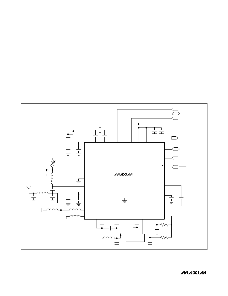
Typical application circuit, Pins and hv, As possible – Rainbow Electronics MAX7032 User Manual
Page 28
MAX7032
Low-Cost, Crystal-Based, Programmable,
ASK/FSK Transceiver with Fractional-N PLL
28
______________________________________________________________________________________
Keeping the traces short also reduces parasitic induc-
tance. Generally, 1in of PC board trace adds about
20nH of parasitic inductance. The parasitic inductance
can have a dramatic effect on the effective inductance
of a passive component. For example, a 0.5in trace
connecting to a 100nH inductor adds an extra 10nH of
inductance, or 10%.
To reduce parasitic inductance, use wider traces and a
solid ground or power plane below the signal traces.
Also, use low-inductance connections to the ground
plane, and place decoupling capacitors as close to all
V
DD
pins and HV
IN
as possible.
1
2
3
4
5
6
7
8
C8
L3
C6
9
10
11
C10
C12
C9
12
L5
C11
13
IN
OUT
GND
14
15
16
Y2
C13
17
18
19
20
21
22
23
24
C17
R1
25
26
27
28
29
30
32
31
CLOCK
OUTPUT
DIO
SCLK
MAX7032
3.0V
C23
V
DD
V
DD
PAV
DD
ROUT
TX/RX1
TX/RX2
PAOUT
AV
DD
LNAIN
LNASRC
LNAOUT
MIXIN+
MIXIN-
IFIN+
IFIN-
PDMIN
PDMAX
MIXOUT
DS-
DS+
OP+
DF
RSSI
T/R
ENABLE
DATA
CLKOUT
DV
DD
HVIN
CS
DIO
SCLK
XT
AL1
XT
AL2
CS
C20
C21
Y1
L4
C14
C15
DATA
ENABLE
C16
TRANSMIT/
RECEIVE
C22
C5
C4
C18
C19
C7
L1
L2
C1
C2
R2
R3*
*OPTIONAL POWER-ADJUST RESISTOR
C24
EXPOSED
PADDLE
C3
L6
V
DD
V
DD
V
DD
Typical Application Circuit