Detailed description, Pin description (continued) – Rainbow Electronics MAX7032 User Manual
Page 13
Detailed Description
The MAX7032 300MHz to 450MHz CMOS transceiver
and a few external components provide a complete
transmit and receive chain from the antenna to the digi-
tal data interface. This device is designed for transmit-
ting and receiving ASK and FSK data. All transmit
frequencies are generated by a fractional-N-based syn-
thesizer, allowing for very fine frequency steps in incre-
ments of f
XTAL
/ 4096. The receive LO is generated by
a traditional integer-N-based synthesizer. Depending
on component selection, data rates as high as 33kbps
(Manchester encoded) or 66kbps (NRZ encoded) can
be achieved.
Receiver
Low-Noise Amplifier (LNA)
The LNA is a cascode amplifier with off-chip inductive
degeneration that achieves approximately 30dB of volt-
age gain that is dependent on both the antenna match-
ing network at the LNA input, and the LC tank network
between the LNA output and the mixer inputs.
The off-chip inductive degeneration is achieved by
connecting an inductor from LNASRC to AGND. This
inductor sets the real part of the input impedance at
LNAIN, allowing for a more flexible match for low-input
impedance such as a PC board trace antenna. A nomi-
nal value for this inductor with a 50
Ω input impedance
is 12nH at 315MHz and 10nH at 434MHz, but the
inductance is affected by PC board trace length.
LNASRC can be shorted to ground to increase sensitiv-
ity by approximately 1dB, but the input match must
then be reoptimized.
The LC tank filter connected to LNAOUT consists of L5
and C9 (see the Typical Application Circuit). Select L5
and C9 to resonate at the desired RF input frequency.
The resonant frequency is given by:
where L
TOTAL
= L5 + L
PARASITICS
and C
TOTAL
= C9 +
C
PARASITICS
.
L
PARASITICS
and C
PARASITICS
include inductance and
capacitance of the PC board traces, package pins,
mixer input impedance, LNA output impedance, etc.
These parasitics at high frequencies cannot be
ignored, and can have a dramatic effect on the tank fil-
ter center frequency. Lab experimentation must be
done to optimize the center frequency of the tank. The
total parasitic capacitance is generally between 5pF
and 7pF.
Automatic Gain Control (AGC)
When the AGC is enabled, it monitors the RSSI output.
When the RSSI output reaches 1.28V, which corre-
sponds to an RF input level of approximately -55dBm,
the AGC switches on the LNA gain-reduction attenua-
tor. The attenuator reduces the LNA gain by 36dB,
thereby reducing the RSSI output by about 540mV to
740mV. The LNA resumes high-gain mode when the
RSSI output level drops back below 680mV (approxi-
mately -59dBm at the RF input) for a programmable
interval called the AGC dwell time. The AGC has a hys-
teresis of approximately 4dB. With the AGC function,
the RSSI dynamic range is increased, allowing the
MAX7032 to reliably produce an ASK output for RF
input levels up to 0dBm with a modulation depth of
18dB. AGC is not required and can be disabled in
either ASK or FSK mode. AGC is not necessary for FSK
mode because large received signal levels do not
affect FSK performance.
f
L
C
TOTAL
TOTAL
=
×
1
2
π
MAX7032
Low-Cost, Crystal-Based, Programmable,
ASK/FSK Transceiver with Fractional-N PLL
______________________________________________________________________________________
13
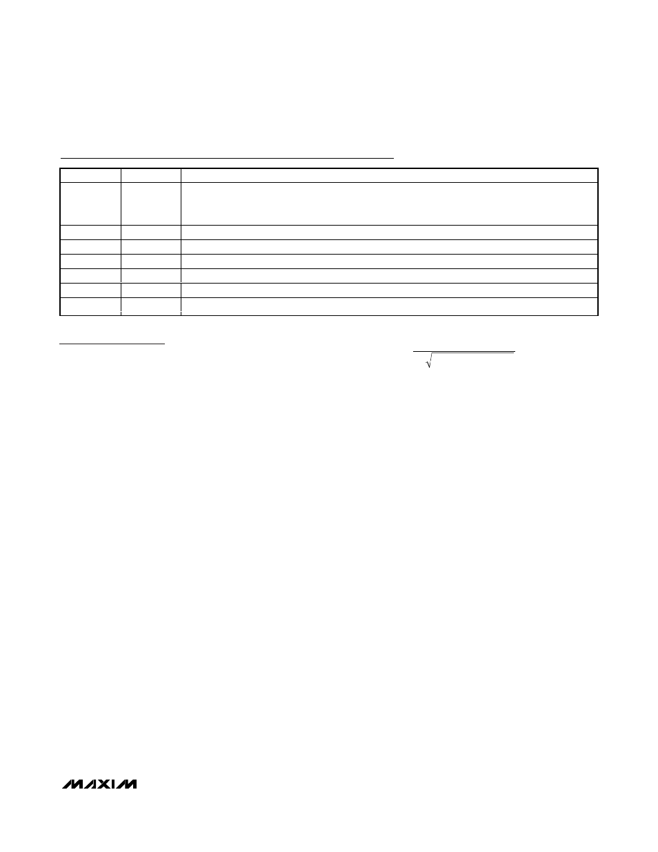
Pin Description (continued)
PIN
NAME
FUNCTION
27
HV
IN
High-Voltage Supply Input. For 3V operation, connect HV
IN
to PAV
DD
, AV
DD
, and DV
DD
.
For 5V
operation, tie only HV
IN
to 5V. Bypass HV
IN
to GND with 0.01µF and 220pF capacitors placed as
close to the pin as possible.
28
CS
Serial Interface Active-Low Chip Select
29
DIO
Serial Interface Serial Data Input/Output
30
SCLK
Serial Interface Clock Input
31
XTAL1
Crystal Input 1. Bypass to GND if XTAL2 is driven by an AC-coupled external reference.
32
XTAL2
Crystal Input 2. XTAL2 can be driven from an AC-coupled external reference.
EP
GND
Exposed Paddle. Solder evenly to the board’s ground plane for proper operation.