Table 2. command bits – Rainbow Electronics MAX7032 User Manual
Page 18

MAX7032
Low-Cost, Crystal-Based, Programmable,
ASK/FSK Transceiver with Fractional-N PLL
18
______________________________________________________________________________________
Crystal Oscillator (XTAL)
The XTAL oscillator in the MAX7032 is designed to pre-
sent a capacitance of approximately 3pF between the
XTAL1 and XTAL2 pins. In most cases, this corre-
sponds to a 4.5pF load capacitance applied to the
external crystal when typical PC board parasitics are
added. It is very important to use a crystal with a
load capacitance that is equal to the capacitance of
the MAX7032 crystal oscillator plus PC board para-
sitics. If a crystal designed to oscillate with a different
load capacitance is used, the crystal is pulled away
from its stated operating frequency, introducing an
error in the reference frequency. Crystals designed to
operate with higher differential load capacitance
always pull the reference frequency higher.
In actuality, the oscillator pulls every crystal. The crys-
tal’s natural frequency is really below its specified fre-
quency, but when loaded with the specified load
capacitance, the crystal is pulled and oscillates at its
specified frequency. This pulling is already accounted
for in the specification of the load capacitance.
Additional pulling can be calculated if the electrical
parameters of the crystal are known. The frequency
pulling is given by:
where:
f
p
is the amount the crystal frequency is pulled in ppm.
C
m
is the motional capacitance of the crystal.
C
CASE
is the case capacitance.
C
SPEC
is the specified load capacitance.
C
LOAD
is the actual load capacitance.
When the crystal is loaded as specified, i.e., C
LOAD
=
C
SPEC
, the frequency pulling equals zero.
Serial Control Interface
Communication Protocol
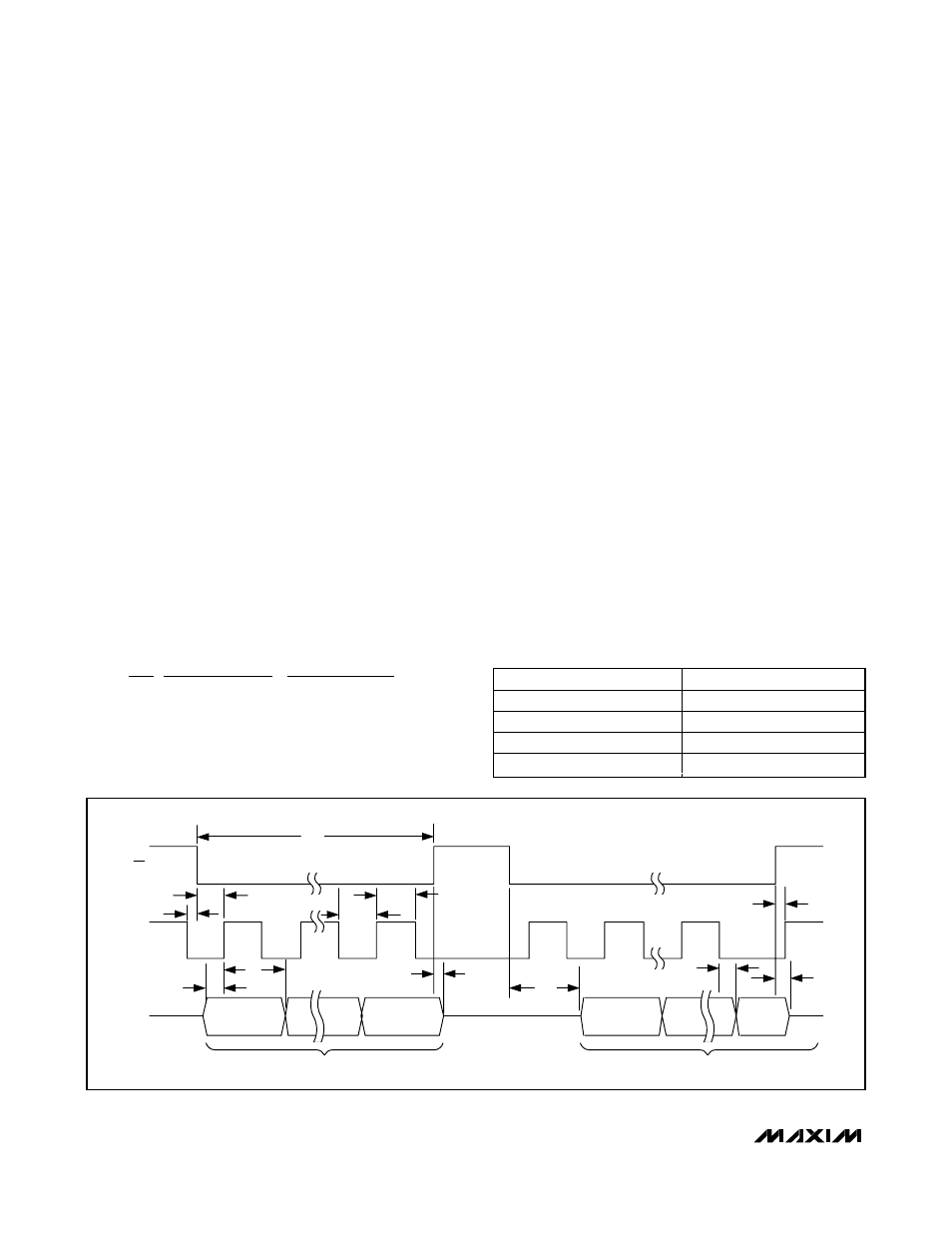
The MAX7032 programs through a 3-wire interface. The
data input must follow the timing diagrams shown in
Figures 7, 8, and 9.
Note that the DIO line must be held LOW while CS is
high. This is to prevent the MAX7032 from entering dis-
continuous receive mode if the DRX bit is high. The
data is latched on the rising edge of SCLK, and there-
fore must be stable before that edge. The data
sequencing is MSB first, the command (C[1:0] see
Table 2), the register address (A[5:0] see Table 3), and
the data (D[7:0] see Table 4).
f
C
C
C
C
C
P
m
CASE
LOAD
CASE
SPEC
=
+
−
+
⎛
⎝⎜
⎞
⎠⎟
×
2
1
1
10
6
C[1:0]
DESCRIPTION
0x0
No operation
0x1
Write data
0x2
Read data
0x3
Master reset
Table 2. Command Bits
HI-Z
DATA OUT
CS
t
CSS
t
DS
t
DH
t
CH
t
CL
t
TH
DATA IN
t
DV
HI-Z
t
DO
t
CSH
t
TR
HI-Z
SCLK
DIO
t
CS
t
SC
D7
D0
Figure 7. Serial Interface Timing Diagram
