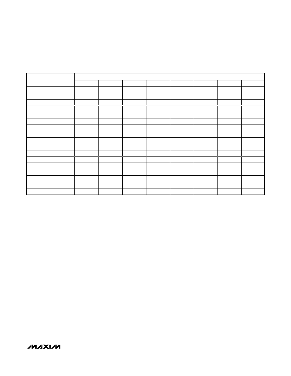
Table 4. register configuration – Rainbow Electronics MAX7032 User Manual
Page 21
MAX7032
Low-Cost, Crystal-Based, Programmable,
ASK/FSK Transceiver with Fractional-N PLL
______________________________________________________________________________________
21
Continuous Receive Mode (DRX = 0)
In continuous receive mode, individual analog modules
can be powered on directly through the power configu-
ration register (register 0x00). The SLEEP bit (bit 0 in
register 0x01) overrides the power configuration regis-
ters and puts the device into deep-sleep mode when
set. It is also necessary to write the frequency divisor of
the external crystal in the oscillator frequency register
(register 0x05) to optimize image rejection and to
enable accurate calibration sequences for the polling
timer and the FSK demodulator. This number is the
integer result of f
XTAL
/ 100kHz.
If the FSK receive function is selected, it is necessary to
perform an FSK calibration to allow operation; other-
wise, the demodulator is saturated. Polling timer cali-
bration is not necessary. See the Calibration section for
more information.
Discontinuous Receive Mode (DRX = 1)
In the discontinuous receive mode (DRX = 1), the
receiver modules set to logic 1 by the power register
(0x00) of the MAX7032 toggle between OFF and ON,
according to internal timers t
OFF
, t
CPU
, t
RF
, and t
ON
. It
is also necessary to write the frequency divisor of the
external crystal in the oscillator frequency register (reg-
ister 0x05). This number is the integer result of f
XTAL
/
100kHz. Before entering the discontinuous receive
mode for the first time, it is also necessary to calibrate
the timers (see the Calibration section).
The MAX7032 uses a series of internal timers (t
OFF
,
t
CPU
, t
RF
, and t
ON
) to control its power-up sequence.
The timer sequence begins when both CS and DIO are
one. The MAX7032 has an internal pullup on the DIO
pin, so the user must tri-state the DIO line when CS
goes high.
The external CPU can then go to a sleep mode during
t
OFF
. A high-to-low transition on DIO, or a low level on
DIO serves as the wake-up signal for the CPU, which
must then start its wake-up procedure, and drive DIO
low before t
LOW
expires (t
CPU
+ t
RF
+ t
ON
). Once t
RF
expires and t
ON
is active, the MAX7032 enables the
data output. The CPU must then keep DIO low for as
long as it may need to analyze any received data.
Releasing DIO after t
ON
expires causes the MAX7032
to pull up DIO, reinitiating the t
OFF
timer.
DATA
NAME (ADDRESS)
D7
D6
D5
D4
D3
D2
D1
D0
POWER[7:0] (0x00)
LNA
AGC
MIXER
BaseB
PkDet
PA
RSSIO
X
CONTRL[7:0] (0x01)
AGCLK
GAIN
TRK_EN
—
PCAL
FCAL
CKOUT
SLEEP
CONF0[7:0] (0x02)
Mode
T/R
MGAIN
DRX
OFPS1
OFPS0
ONPS1
ONPS0
CONF1[7:0] (0x03)
—
ACAL
CLKOF
CDIV1
CDIV0
DT2
DT1
DT0
OSC[7:0] (0x05)
OSC7
OSC6
OSC5
OSC4
OSC3
OSC2
OSC1
OSC0
t
OFF
[15:8] (0x06)
t
OFF
15
t
OFF
14
t
OFF
13
t
OFF
12
t
OFF
11
t
OFF
10
t
OFF
9
t
OFF
8
t
OFF
[7:0] (0x07)
t
OFF
7
t
OFF
6
t
OFF
5
t
OFF
4
t
OFF
3
t
OFF
2
t
OFF
1
t
OFF
0
t
CPU
[7:0] (0x08)
t
CPU
7
t
CPU
6
t
CPU
5
t
CPU
4
t
CPU
3
t
CPU
2
t
CPU
1
t
CPU
0
t
RF
[15:8] (0x09)
t
RF
15
t
RF
14
t
RF
13
t
RF
12
t
RF
11
t
RF
10
t
RF
9
t
RF
8
t
RF
[7:0] (0x0A)
t
RF
7
t
RF
6
t
RF
5
t
RF
4
t
RF
3
t
RF
2
t
RF
1
t
RF
0
t
ON
[15:8] (0x0B)
t
ON
15
t
ON
14
t
ON
13
t
ON
12
t
ON
11
t
ON
10
t
ON
9
t
ON
8
t
ON
[7:0] (0x0C)
t
ON
7
t
ON
6
t
ON
5
t
ON
4
t
ON
3
t
ON
2
t
ON
1
t
ON
0
TxLOW[15:8] (0x0D)
TxL15
TxL14
TxL13
TxL12
TxL11
TxL10
TxL9
TxL8
TxLOW[7:0] (0x0E)
TxL7
TxL6
TxL5
TxL4
TxL3
TxL2
TxL1
TxL0
TxHIGH[15:8] (0x0F)
TxH15
TxH14
TxH13
TxH12
TxH11
TxH10
TxH9
TxH8
TxHIGH[7:0] (0x10)
TxH7
TxH6
TxH5
TxH4
TxH3
TxH2
TxH1
TxH0
STATUS[7:0] (0x1A)
LCKD
GAINS
CLKON
0
0
0
PCALD
FCALD
Table 4. Register Configuration