Pin description – Rainbow Electronics MAX7032 User Manual
Page 12
MAX7032
Low-Cost, Crystal-Based, Programmable,
ASK/FSK Transceiver with Fractional-N PLL
12
______________________________________________________________________________________
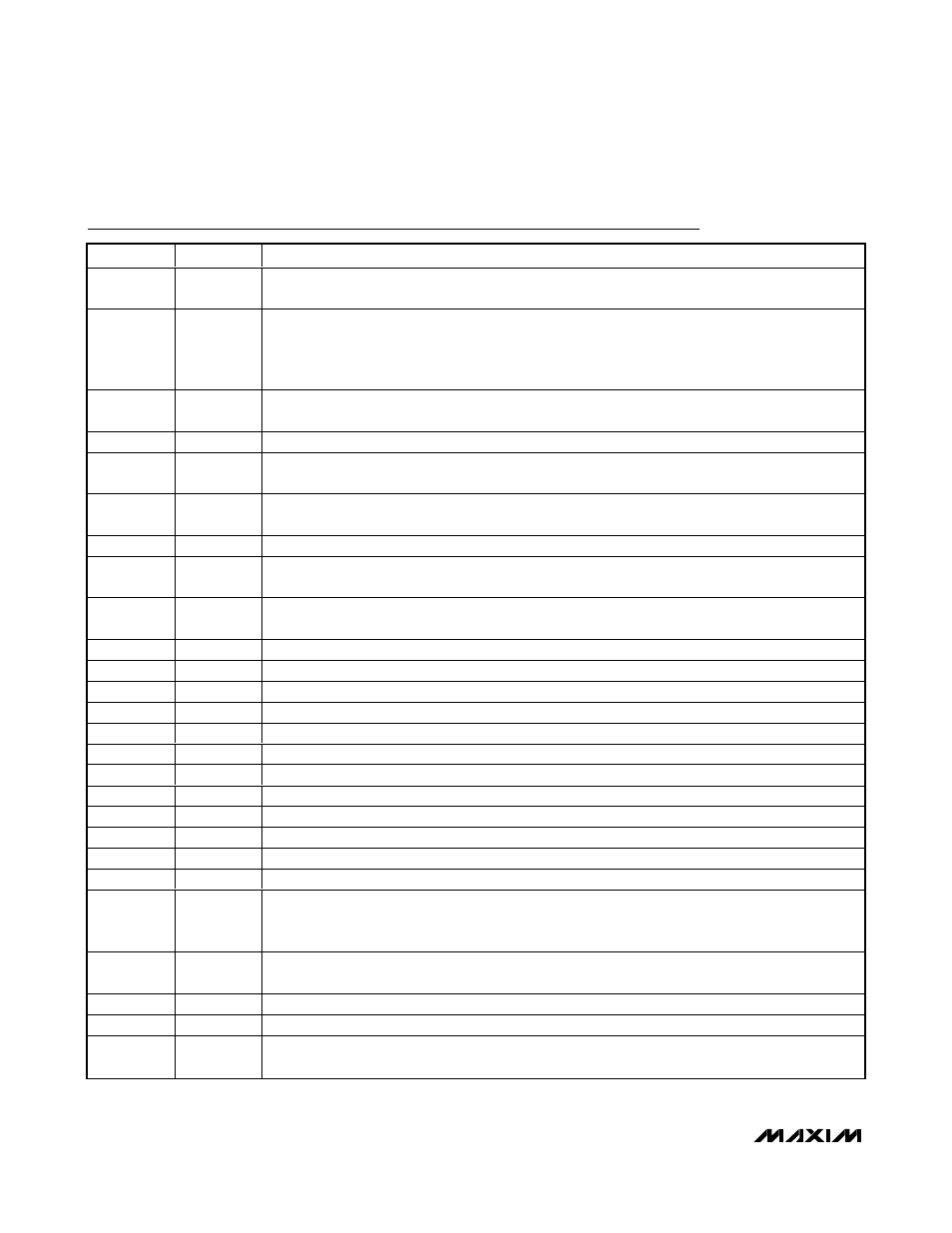
Pin Description
PIN
NAME
FUNCTION
1
PAV
DD
Power-Amplifier Supply Voltage. Bypass to GND with 0.01µF and 220pF capacitors placed as close
to the pin as possible.
2
ROUT
Envelope-Shaping Output. ROUT controls the power-amplifier envelope’s rise and fall times. Connect
ROUT to the PA pullup inductor or optional power-adjust resistor. Bypass the inductor to GND as
close to the inductor as possible with 680pF and 220pF capacitors as shown in the Typical
Application Circuit.
3
TX/RX1
Transmit/Receive Switch Throw. Drive T/R high to short TX/RX1 to TX/RX2. Drive T/R low to disconnect
TX/RX1 from TX/RX2. Functionally identical to TX/RX2.
4
TX/RX2
Transmit/Receive Switch Pole. Typically connected to ground. See the Typical Application Circuit.
5
PAOUT
Power-Amplifier Output. Requires a pullup inductor to the supply voltage (or ROUT if envelope
shaping is desired), which may be part of the output-matching network to an antenna.
6
AV
DD
Analog Power-Supply Voltage. AV
DD
is connected to an on-chip +3.0V regulator in 5V operation.
Bypass AV
DD
to GND with 0.1µF and 220pF capacitors placed as close to the pin as possible.
7
LNAIN
Low-Noise Amplifier Input. Must be AC-coupled.
8
LNASRC
Low-Noise Amplifier Source for External Inductive Degeneration. Connect an inductor to GND to set
the LNA input impedance.
9
LNAOUT
Low-Noise Amplifier Output. Must be tied to AV
DD
through a parallel LC tank filter. AC-couple to
MIXIN+.
10
MIXIN+
Noninverting Mixer Input. Must be AC-coupled to the LNA output.
11
MIXIN-
Inverting Mixer Input. Bypass to AV
DD
with a capacitor as close to LNA LC tank filter as possible.
12
MIXOUT
330
Ω Mixer Output. Connect to the input of the 10.7MHz filter.
13
IFIN-
Inverting 330
Ω IF Limiter Amplifier Input. Bypass to GND with a capacitor.
14
IFIN+
Noninverting 330
Ω IF Limiter Amplifier Input. Connect to the output of the 10.7MHz IF filter.
15
PDMIN
Minimum-Level Peak Detector for Demodulator Output
16
PDMAX
Maximum-Level Peak Detector for Demodulator Output
17
DS-
Inverting Data Slicer Input
18
DS+
Noninverting Data Slicer Input
19
OP+
Noninverting Op Amp Input for the Sallen-Key Data Filter
20
DF
Data Filter Feedback Node. Input for the feedback of the Sallen-Key data filter.
21
RSSI
Buffered Received-Signal-Strength Indicator Output
22
T/R
Transmit/ Receive. Drive high to put the device in transmit mode. Drive low or leave unconnected to
put the device in receive mode. It is internally pulled down. This function is also controlled by a
configuration register.
23
ENABLE
Enable. Drive high for normal operation. Drive low or leave unconnected to put the device into
shutdown mode.
24
DATA
Receiver Data Output/Transmitter Data Input
25
CLKOUT
Divided Crystal Clock Buffered Output
26
DV
DD
Digital Power-Supply Voltage. Bypass to GND with 0.01µF and 220pF capacitors placed as close to
the pin as possible.