Electrical characteristics (continued) – Rainbow Electronics MAX17409 User Manual
Page 7
MAX17409
1-Phase Quick-PWM GPU Controller
_______________________________________________________________________________________
7
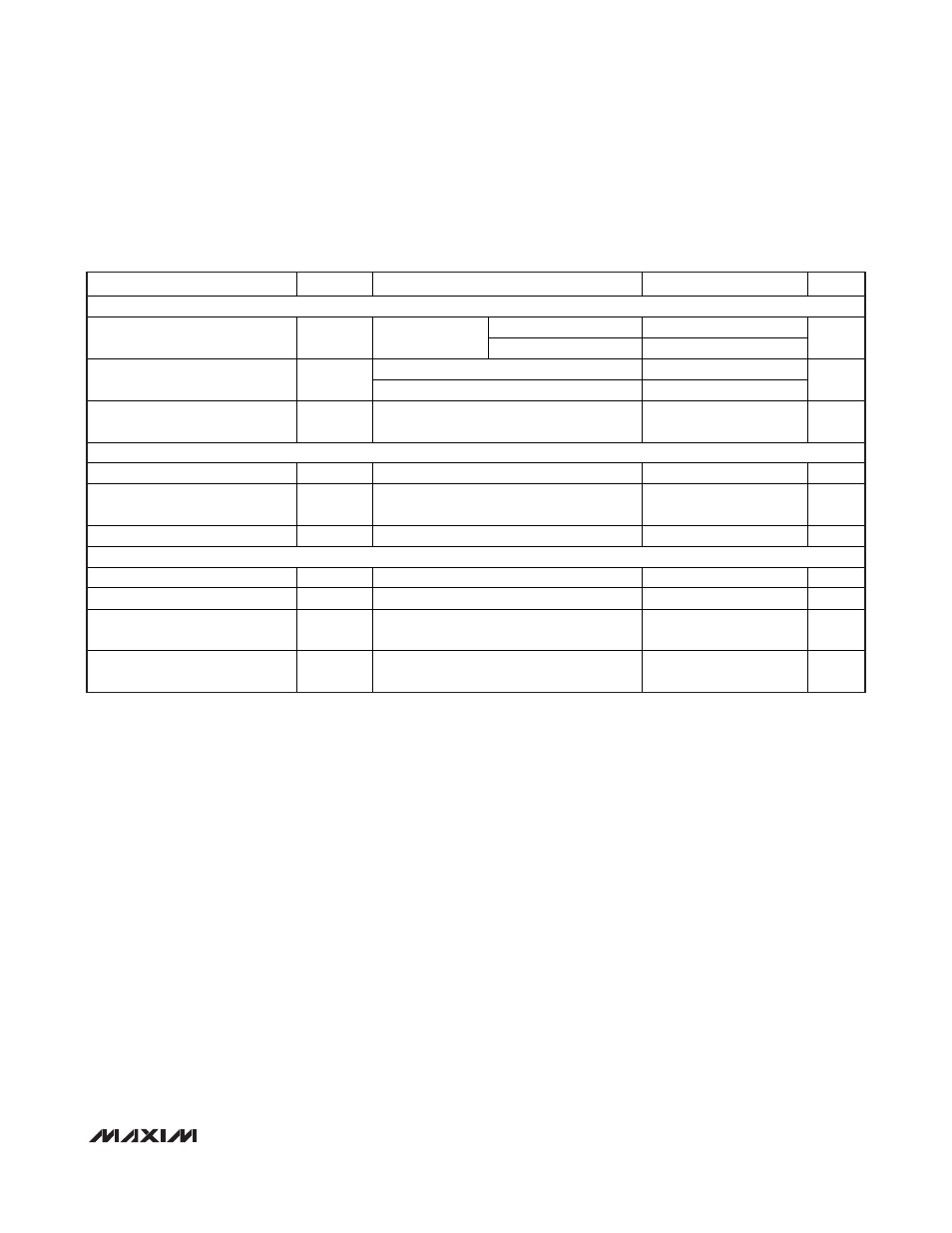
ELECTRICAL CHARACTERISTICS (continued)
(Circuit of Figure 1, V
IN
= 12V, V
DD
= V
CC
= 5V, SHDN = ILIM = V
CC
, SKIP = GNDS = PGND = GND, V
FB
= V
CSP
= V
CSN
= 1.05V;
G5–G0 set for 1.05V (G0–G5 = 100110); T
A
= -40
°C to +105°C, unless otherwise specified.) (Note 3)
PARAMETER
SYMBOL
CONDITIONS
MIN
TYP
MAX
UNITS
GATE DRIVERS
High state (pullup)
2.5
DH Gate-Driver On-Resistance
R
ON(DH)
BST - LX forced
to 5V
Low state (pulldown)
2.0
High state (pullup)
2.0
DL Gate-Driver On-Resistance
R
ON(DL)
Low state (pulldown)
0.7
Internal BST Switch
On-Resistance
R
BST
I
BST
= 10mA, V
DD
= 5V
20
CURRENT MONITOR
Current-Monitor Transconductance
G
m(IMON)
I
IMON
/
(V
CSP
- V
CSN
) V
CSN
= 0.5V to 1.0V
4.9
5.1
mS
Current-Monitor Offset Referred
to V(CSP,CSN)
I
IMON
= 0
-1.0
+1.0
mV
IMON Clamp Voltage
V
IMON
I
IMON
= -1.0mA
1.05
1.15
V
LOGIC AND I/O
Logic-Input High Voltage
V
IH
SHDN, SKIP
2.3
V
Logic-Input Low Voltage
V
IL
SHDN, SKIP
1.0
V
Low-Voltage Logic-Input
High Voltage
V
IHLV
G0–G5 0.67
V
Low-Voltage Logic-Input
Low Voltage
V
ILLV
G0–G5
0.33
V
Note 3: Limits are 100% production tested at T
A
= +25°C. Maximum and minimum limits over temperature are guaranteed by design
and characterization.
Note 4: The equation for the target voltage V
TARGET
is:
V
TARGET
= the slew-rate-controlled version of V
DAC
, where V
DAC
= 0 for shutdown, V
DAC
= V
VID
otherwise (the V
VID
volt-
ages for all possible VID codes are given in Table 4).
In pulse-skipping mode, the output rises by approximately 1.5% when transitioning from continuous conduction to no load.
Note 5: On-time and minimum off-time specifications are measured from 50% to 50% at the DH pin, with LX forced to 0V, BST forced
to 5V, and a 500pF capacitor from DH to LX to simulate external MOSFET gate capacitance. Actual in-circuit times might be
different due to MOSFET switching speeds.