Electrical characteristics (continued) – Rainbow Electronics MAX17409 User Manual
Page 3
MAX17409
1-Phase Quick-PWM GPU Controller
_______________________________________________________________________________________
3
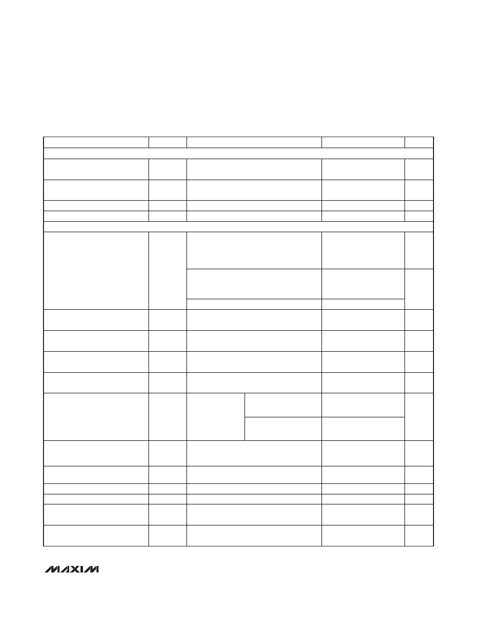
PARAMETER SYMBOL
CONDITIONS
MIN
TYP
MAX
UNITS
BIAS CURRENTS
Quiescent Supply Current (V
CC
) I
CC
Measured at V
CC
, SKIP = 5V, FB forced
above the regulation point
1.5 3 mA
Quiescent Supply Current (V
DD
) I
DD
Measured at V
DD
, SKIP = 0V, FB forced
above the regulation point, T
A
= +25°C
0.02 1 µA
Shutdown Supply Current (V
CC
)
Measured at V
CC
,
SHDN = GND, T
A
= +25°C
0.01
1
µA
Shutdown Supply Current (V
DD
)
Measured at V
DD
,
SHDN = GND, T
A
= +25°C
0.01
1
µA
FAULT PROTECTION
Skip mode after output reaches the
regulation voltage or PWM mode;
measured at FB with respect to unloaded
output voltage
250 300 350 mV
Soft-start, soft-shutdown, skip mode, and
output have not reached the regulation
voltage; measured at FB
1.45 1.50 1.55
Output Overvoltage Protection
Threshold
V
OVP
Minimum OVP threshold; measured at FB
0.8
V
Output Overvoltage Propagation
Delay
t
OVP
FB forced 25mV above trip threshold
10
µs
Output Undervoltage Protection
Threshold
V
UVP
Measured at FB with respect to unloaded
output voltage
-450 -400 -350 mV
Output Undervoltage
Propagation Delay
t
UVP
FB forced 25mV below trip threshold
10
µs
PWRGD Startup Delay
Measured at startup from the time when
SHDN goes high
3 5 8 ms
Lower threshold, falling
edge (undervoltage)
-350 -300 -250
PWRGD Threshold
Measured at FB
with respect to
unloaded output
voltage, 15mV
hysteresis (typ)
Upper threshold, rising
edge (overvoltage)
+150 +200 +250
mV
PWRGD Transition Blanking
Time
t
BLANK
Measured from the time when FB reaches
the target voltage (Note 4) based on the
slew rate
20 µs
PWRGD Delay
FB forced 25mV outside the PWRGD trip
thresholds
10 µs
PWRGD Output Low Voltage
I
SINK
= 3mA
0.4
V
PWRGD Leakage Current
High state, PWRGD forced to 5V
1
µA
V
CC
Undervoltage-Lockout
Threshold
V
UVLO(VCC)
Rising edge, 50mV typical hysteresis,
controller disabled below this level
4.05 4.25 4.48 V
CSN Discharge Resistance
in UVLO
V
CC
= V
DD
=
4.0V
8
ELECTRICAL CHARACTERISTICS (continued)
(Circuit of Figure 1, V
IN
= 12V, V
DD
= V
CC
= 5V, SHDN = ILIM = V
CC
, SKIP = GNDS = PGND = GND, V
FB
= V
CSP
= V
CSN
= 1.05V;
G5–G0 set for 1.05V (G0–G5 = 100110); T
A
= 0
°C to +85°C, unless otherwise specified. Typical values are at T
A
= +25°C.) (Note 3)