Rainbow Electronics MAX17409 User Manual
Page 28

MAX17409
1-Phase Quick-PWM GPU Controller
28
______________________________________________________________________________________
In applications that require DC droop, R
DROOP(AC)
is
the same as the DC droop setting (R
DROOP(AC)
=
R
DROOP(DC)
). In applications that do not require DC
droop, this AC signal is generated by capacitively cou-
pling the inductor ripple current signal to the FB pin. In
this case, R
DROOP(AC)
= R
SENSE
, where R
SENSE
is the
effective sense resistance seen at the CSP-CSN pins.
In Figure 1, C3 couples the inductor ripple current signal
to the FB pin. C3 can be connected to the CSN pin or the
CSP pin. Connecting to the CSN pin only couples the out-
put capacitor ESR to the FB pin. Connecting to the CSP
pin adds the R
SENSE
component to the effective resis-
tance in addition to the output capacitor ESR. This is use-
ful for applications using all ceramic output capacitors.
Keep the C3 x R
FB
time constant between 3x and 5x of
the switching period. Practical values for C3 range from
0.1µF to 1µF. Calculate R
FB
after selecting C3. Keeping
R
FB
below 100
Ω minimizes any residual DC droop.
In the standard application circuit (Figure 1), the effec-
tive resistance for stability is the sum of the ~ 2m
Ω DCR
and the 6m
Ω ESR of the 470µF output capacitor. The
ESR zero frequency is 42kHz, well within the require-
ment of f
SW
/
π.
Ceramic capacitors have a high-ESR zero frequency,
but applications with significant voltage positioning can
take advantage of their size and low ESR. Do not put
high-value ceramic capacitors directly across the out-
put without verifying that the circuit contains enough
voltage positioning and series PCB resistance to
ensure stability. When only using ceramic output
capacitors, output overshoot (V
SOAR
) typically deter-
mines the minimum output capacitance requirement.
Their relatively low capacitance value can cause output
overshoot when stepping from full-load to no-load con-
ditions, unless a small inductor value is used (high
switching frequency) to minimize the energy transferred
from inductor to capacitor during load-step recovery.
Unstable operation manifests itself in two related but
distinctly different ways: double-pulsing and feedback
loop instability. Double-pulsing occurs due to noise on
the output or because the ESR is so low that there is not
enough voltage ramp in the output-voltage signal. This
“fools” the error comparator into triggering a new cycle
immediately after the minimum off-time period has
expired. Double-pulsing is more annoying than harmful,
resulting in nothing worse than increased output ripple.
However, it can indicate the possible presence of loop
instability due to insufficient ESR. Loop instability can
result in oscillations at the output after line or load
steps. Such perturbations are usually damped, but can
cause the output voltage to rise above or fall below the
tolerance limits.
The easiest method for checking stability is to apply a
very fast zero-to-max load transient and carefully
observe the output-voltage ripple envelope for over-
shoot and ringing. It can help to simultaneously monitor
the inductor current with an AC current probe. Do not
allow more than one cycle of ringing after the initial
step-response under/overshoot.
Input Capacitor Selection
The input capacitor must meet the ripple current
requirement (I
RMS
) imposed by the switching currents.
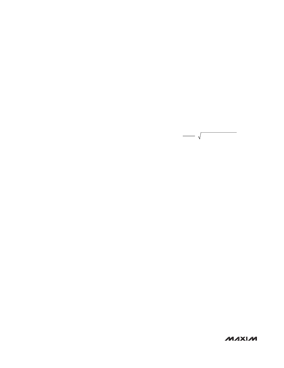
The I
RMS
requirements can be determined by the fol-
lowing equation:
The worst-case RMS current requirement occurs when
operating with V
IN
= 2V
OUT
. At this point, the above
equation simplifies to I
RMS
= 0.5 x I
LOAD
.
For most applications, nontantalum chemistries (ceram-
ic, aluminum, or OS-CON) are preferred due to their
resistance to inrush surge currents typical of systems
with a mechanical switch or connector in series with the
input. If the Quick-PWM controller is operated as the
second stage of a two-stage power-conversion system,
tantalum input capacitors are acceptable. In either con-
figuration, choose an input capacitor that exhibits less
than +10
°C temperature rise at the RMS input current
for optimal circuit longevity.
Power-MOSFET Selection
Most of the following MOSFET guidelines focus on the
challenge of obtaining high load-current capability
when using high-voltage (> 20V) AC adapters. Low-
current applications usually require less attention.
The high-side MOSFET (N
H
) must be able to dissipate the
resistive losses plus the switching losses at both V
IN(MIN)
and V
IN(MAX)
. Calculate both of these sums. Ideally, the
losses at V
IN(MIN)
should be roughly equal to losses at
V
IN(MAX)
, with lower losses in between. If the losses at
V
IN(MIN)
are significantly higher than the losses at
V
IN(MAX)
, consider increasing the size of N
H
(reducing
R
DS(ON)
but with higher C
GATE
). Conversely, if the losses
at V
IN(MAX)
are significantly higher than the losses at
V
IN(MIN)
, consider reducing the size of N
H
(increasing
R
DS(ON)
to lower C
GATE
). If V
IN
does not vary over a wide
range, the minimum power dissipation occurs where the
resistive losses equal the switching losses.
Choose a low-side MOSFET that has the lowest possible
on-resistance (R
DS(ON)
), comes in a moderate-sized
package (i.e., one or two 8-pin SOs, DPAK, or D
2
PAK),
and is reasonably priced. Make sure that the DL gate
I
I
V
V
V
V
RMS
LOAD
IN
OUT
IN
OUT
=
⎛
⎝⎜
⎞
⎠⎟
(
)
-
