Quick-pwm design procedure – Rainbow Electronics MAX17409 User Manual
Page 25
MAX17409
1-Phase Quick-PWM GPU Controller
______________________________________________________________________________________
25
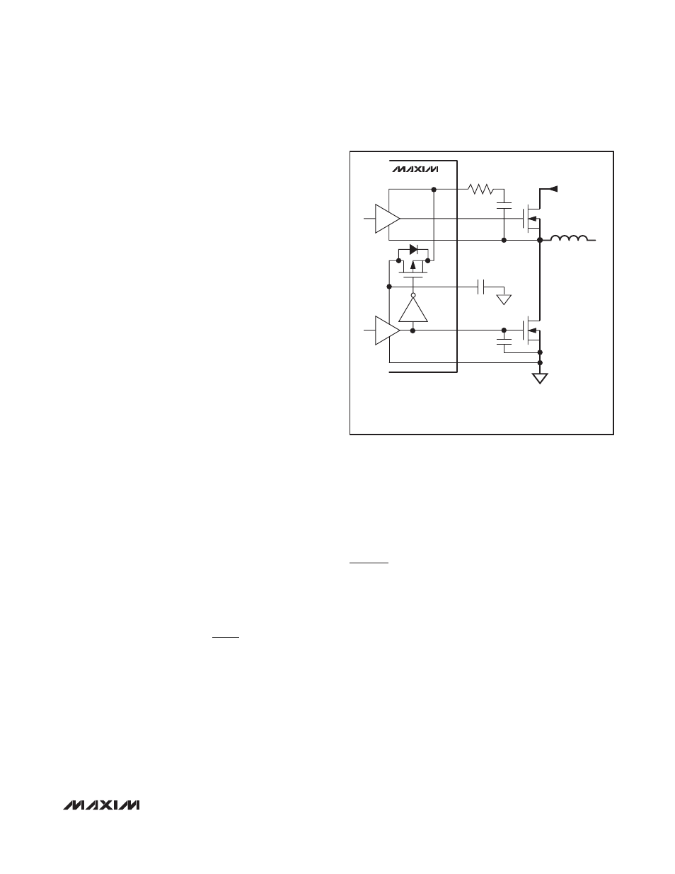
MOSFET Gate Drivers
The DH and DL drivers are optimized for driving moder-
ate-sized high-side and larger low-side power
MOSFETs. This is consistent with the low duty factor
seen in notebook applications, where a large V
IN
-
V
OUT
differential exists. The high-side gate drivers (DH)
source and sink 2.2A, and the low-side gate drivers
(DL) source 2.7A and sink 8A. This ensures robust gate
drive for high-current applications. The DH floating
high-side MOSFET drivers are powered by internal
boost switch charge pumps at BST, while the DL syn-
chronous-rectifier drivers are powered directly by the
5V bias supply (V
DD
).
Adaptive dead-time circuits monitor the DL and DH dri-
vers and prevent either FET from turning on until the
other is fully off. The adaptive driver dead-time allows
operation without shoot-through with a wide range of
MOSFETs, minimizing delays and maintaining efficiency.
There must be a low-resistance, low-inductance path
from the DL and DH drivers to the MOSFET gates for
the adaptive dead-time circuits to work properly; other-
wise, the sense circuitry in the MAX17409 interprets the
MOSFET gates as “off” while charge actually remains.
Use very short, wide traces (50 mils to 100 mils wide if
the MOSFET is 1in from the driver).
The internal pulldown transistor that drives DL low is
robust, with a 0.25
Ω (typ) on-resistance. This helps DL
from being pulled up due to capacitive coupling from
the drain to the gate of the low-side MOSFETs when the
inductor node (LX) quickly switches from ground to V
IN
.
Applications with high input voltages and long inductive
driver traces might require that rising LX edges do not
pull up the low-side MOSFETs’ gate, causing shoot-
through currents. The capacitive coupling between LX
and DL created by the MOSFET’s gate-to-drain capaci-
tance (C
RSS
), gate-to-source capacitance (C
ISS
-
C
RSS
), and additional board parasitics should not
exceed the following minimum threshold:
Typically, adding a 4700pF between DL and power
ground (C
NL
in Figure 7), close to the low-side
MOSFETs, greatly reduces coupling. Do not exceed
22nF of total gate capacitance to prevent excessive
turn-off delays.
Alternatively, shoot-through currents could be caused
by a combination of fast high-side MOSFETs and slow
low-side MOSFETs. If the turn-off delay time of the low-
side MOSFET is too long, the high-side MOSFETs can
turn on before the low-side MOSFETs have actually
turned off. Adding a resistor less than 5
Ω in series with
BST slows down the high-side MOSFET turn-on time,
eliminating the shoot-through currents without degrad-
ing the turn-off time (R
BST
in Figure 7). Slowing down
the high-side MOSFET also reduces the LX node rise
time, thereby reducing EMI and high-frequency cou-
pling responsible for switching noise.
Quick-PWM Design Procedure
Firmly establish the input voltage range and maximum
load current before choosing a switching frequency
and inductor operating point (ripple-current ratio). The
primary design trade-off lies in choosing a good switch-
ing frequency and inductor operating point, and the fol-
lowing four factors dictate the rest of the design:
•
Input voltage range: The maximum value
(V
IN(MAX)
) must accommodate the worst-case high
AC adapter voltage. The minimum value (V
IN(MIN)
)
must account for the lowest input voltage after
drops due to connectors, fuses, and battery selec-
tor switches. If there is a choice at all, lower input
voltages result in better efficiency.
•
Maximum load current: There are two values to
consider. The peak load current (I
LOAD(MAX)
) deter-
mines the instantaneous component stresses and
filtering requirements, and thus drives output
V
V
C
C
GS TH
IN
RSS
ISS
(
)
>
⎛
⎝⎜
⎞
⎠⎟
BST
DH
LX
INPUT (V
IN
)
N
H
C
BST
(C
NL
)*
C
BYP
(R
BST
)*
N
L
L
(R
BST
)* OPTIONAL—THE RESISTOR LOWERS EMI, DECREASING THE
SWITCHING NODE RISE TIME.
(C
NL
)* OPTIONAL—THE CAPACITOR REDUCES LX TO DL CAPACITIVE
COUPLING THAT CAN CAUSE SHOOT-THROUGH CURRENTS.
DL
PGND
V
DD
MAX17409
Figure 7. Gate-Drive Circuit