Rainbow Electronics MAX17409 User Manual
Page 2
MAX17409
1-Phase Quick-PWM GPU Controller
2
_______________________________________________________________________________________
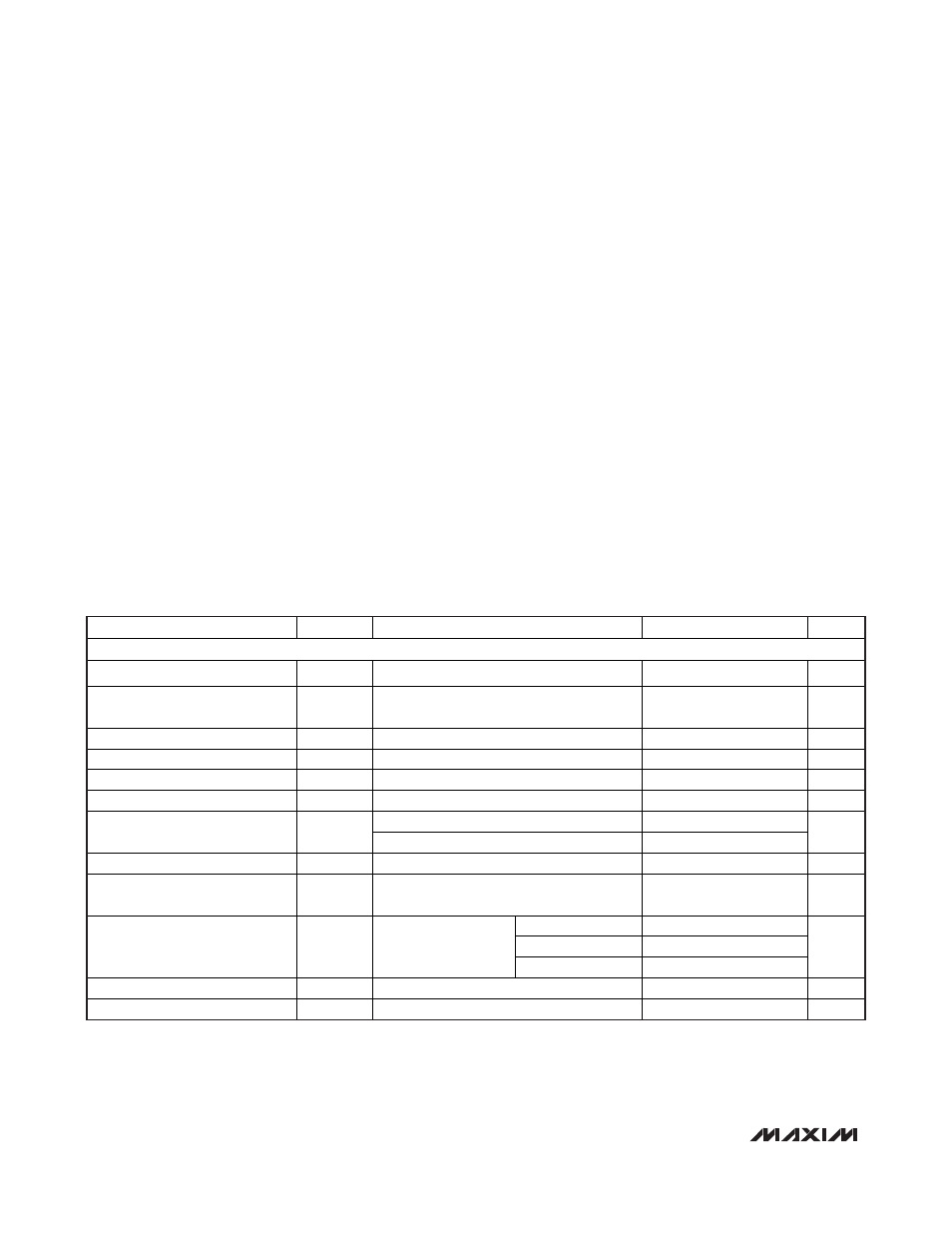
ABSOLUTE MAXIMUM RATINGS
ELECTRICAL CHARACTERISTICS
(Circuit of Figure 1, V
IN
= 12V, V
DD
= V
CC
= 5V, SHDN = ILIM = V
CC
, SKIP = GNDS = PGND = GND, V
FB
= V
CSP
= V
CSN
= 1.05V;
G5–G0 set for 1.05V (G0–G5 = 100110); T
A
= 0
°C to +85°C, unless otherwise specified. Typical values are at T
A
= +25°C.) (Note 3)
Stresses beyond those listed under “Absolute Maximum Ratings” may cause permanent damage to the device. These are stress ratings only, and functional
operation of the device at these or any other conditions beyond those indicated in the operational sections of the specifications is not implied. Exposure to
absolute maximum rating conditions for extended periods may affect device reliability.
V
CC
, V
DD
to GND .....................................................-0.3V to +6V
G0–G5 to GND .........................................................-0.3V to +6V
CSP, CSN to GND ....................................................-0.3V to +6V
ILIM, THRM, VRHOT, PWRGD to GND ....................-0.3V to +6V
SKIP to GND.............................................................-0.3V to +6V
CCV, FB, IMON, REF to GND .....................-0.3V to (V
CC
+ 0.3V)
SHDN to GND (Note 1)...........................................-0.3V to +30V
TON to GND ...........................................................-0.3V to +30V
GNDS/OFSP, PGND to GND (Note 2) ...................-0.3V to +0.3V
Internal Driver (Note 2)
DL to PGND .............................................-0.3V to (V
DD
+ 0.3V)
BST to GND .........................................................-0.3V to +36V
LX to BST...............................................................-6V to +0.3V
BST to V
DD
..........................................................-0.3V to +30V
DH to LX .................................................-0.3V to (V
BST
+ 0.3V)
Continuous Power Dissipation (T
A
= +70°C)
28-Pin 4mm x 4mm TQFN
(derate 21.3mW/°C above +70°C) ............................1702mW
Operating Temperature Range .........................-40°C to +105°C
Junction Temperature ......................................................+150°C
Storage Temperature Range .............................-65°C to +165°C
Lead Temperature (soldering, 10s) .................................+300°C
PARAMETER
SYMBOL
CONDITIONS
MIN
TYP
MAX
UNITS
PWM CONTROLLER
Input Voltage Range
V
CC
, V
DD
4.5
5.5
V
DC Output-Voltage Accuracy
Measured at FB with respect to GNDS;
includes load-regulation error (Note 4)
-6 +6
mV
Line Regulation Error
V
CC
= 4.5V to 5.5V, V
IN
= 4.5V to 26V
0.1
%
GNDS Input Range
-200
+200
mV
GNDS/OFSP Gain
A
GNDS
V
OUT
/
V
GNDS
, -200mV
V
GNDS
+200mV
0.97 1.00 1.03 V/V
GNDS/OFSP Input Bias Current
I
GNDS
-2
+2
µA
V
CC
= 4.5V to 5.5V, I
REF
= 100µA
1.98
2.000
2.02
REF Voltage
V
REF
I
REF
= 0 to 1mA
1.97
2.000
2.02
V
Dynamic VID Slew-Rate Accuracy
11.0
12.5
14.0
mV/µs
Soft-Start/Soft-Shutdown
Slew-Rate Accuracy
1.248
1.56
1.872
mV/µs
R
TON
= 96.75k
142 167 192
R
TON
= 200k
300 333 366
On-Time (Note 5)
t
ON
V
IN
= 12V, V
FB
= 1.2V
R
TON
= 303.25k
425 500 575
ns
Minimum Off-Time
t
OFF(MIN)
Measured at DH (Note 5)
300
375
ns
TON Shutdown Input Current
SHDN = GND, V
IN
= 26V, V
CC
= V
DD
= 0 or 5V
0.01
0.1
µA
Note 1: SHDN might be forced to 12V for the purpose of debugging prototype breadboards using the no-fault test mode, which dis-
ables fault protection.
Note 2: Measurements valid using a 20MHz bandwidth limit.